- 您现在的位置:买卖IC网 > PDF目录293971 > 5962D1022901QXC 64M X 40 SYNCHRONOUS DRAM, 5.4 ns, CQFP128 PDF资料下载
参数资料
| 型号: | 5962D1022901QXC |
| 元件分类: | DRAM |
| 英文描述: | 64M X 40 SYNCHRONOUS DRAM, 5.4 ns, CQFP128 |
| 封装: | CERAMIC, QFP-128 |
| 文件页数: | 16/68页 |
| 文件大小: | 1475K |
| 代理商: | 5962D1022901QXC |
第1页第2页第3页第4页第5页第6页第7页第8页第9页第10页第11页第12页第13页第14页第15页当前第16页第17页第18页第19页第20页第21页第22页第23页第24页第25页第26页第27页第28页第29页第30页第31页第32页第33页第34页第35页第36页第37页第38页第39页第40页第41页第42页第43页第44页第45页第46页第47页第48页第49页第50页第51页第52页第53页第54页第55页第56页第57页第58页第59页第60页第61页第62页第63页第64页第65页第66页第67页第68页
23
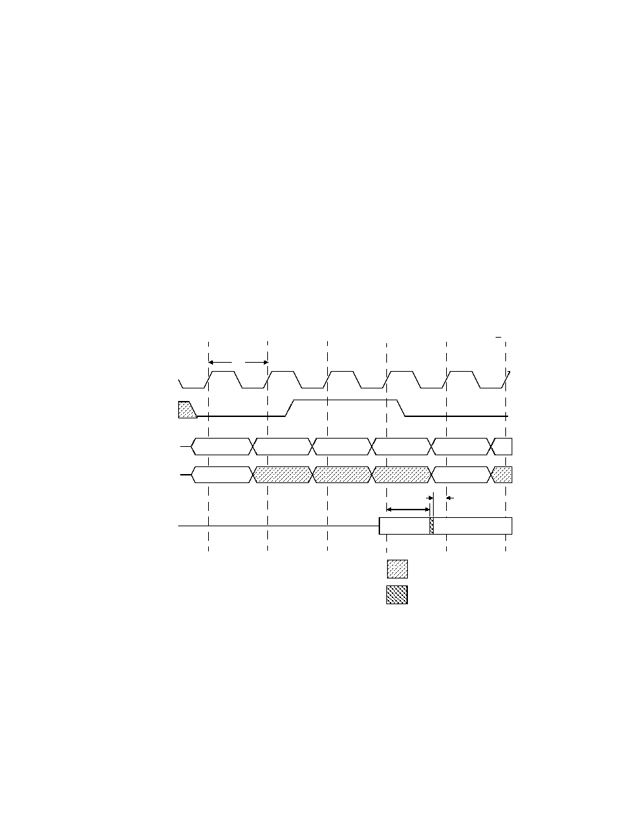
Data from any READ burst may be truncated with a subsequent WRITE command, and data from a fixed-length READ burst may
be immediately followed by data from a WRITE command (subject to bus turnaround limitations). The WRITE burst may be
initiated on the clock edge immediately following the last (or last desired) data element from the READ burst, provided that I/O
contention can be avoided. In a given system design, there may be a possibility that the device driving the input data will go Low-Z
before the SDRAM DQs go High-Z. In this case, at least a single-cycle delay should occur between the last read data and the
WRITE command.
The DQM input is used to avoid I/O contention, as shown in Figure 12 and Figure 13. The DQM signal must be asserted (HIGH) at
least two clocks prior to the WRITE command (DQM latency is two clocks for output buffers) to suppress dataout from the READ.
After the WRITE command is registered, the DQs go High-Z (or remain High-Z), regardless of the state of the DQM signal,
provided the DQM was active on the clock just prior to the WRITE command that truncated the READ command. If not, the second
WRITE will be an invalid WRITE. For example, if DQM was LOW during T4 in Figure 13, then the WRITEs at T5 and T7 would
be valid, while the WRITE at T6 would be invalid.
The DQM signal must be de-asserted prior to the WRITE command (DQM latency is zero clocks for input buffers) to ensure that the
written data is not masked. Figure 12 shows the case where the clock frequency allows for bus contention to be avoided without add-
ing a NOP cycle, and Figure 13 shows the case where the additional NOP is needed.
Figure 12: READ-to-WRITE
READ
NOP
WRITE
BANK
Dout n
Din b
T5
T4
T3
T2
T1
T0
tHZ
tDS
tCK
Notes:
1.
CL = 3 is used for illustration. The READ or WRITE Command may be to any bank.
CLK
DQM
Command
Address
DQ
If a burst of one is used, DQM is not required.
Don’t Care
Transitioning Data
COL n
BANK
COL b
相关PDF资料 |
PDF描述 |
|---|---|
| 5962F0253401VXC | 2.5 V FIXED POSITIVE REGULATOR, CDFP16 |
| L491333DIE2V | 3.3 V FIXED POSITIVE REGULATOR, UUC |
| 5962F9654403QXA | OTHER DECODER/DRIVER, CDFP16 |
| 5962F9657601QCX | AC SERIES, 4-BIT LOOK-AHEAD CARRY GENERATOR, TRUE OUTPUT, CDIP16 |
| 5962F9657701VXC | ACT SERIES, 4-BIT LOOK-AHEAD CARRY GENERATOR, TRUE OUTPUT, CDFP16 |
相关代理商/技术参数 |
参数描述 |
|---|---|
| 5962D9563201VXC | 制造商:STMicroelectronics 功能描述:RS-432LINE DRIVERQUADFLAT16, GOLD - Bulk |
| 5962D9666301VXC | 制造商:STMicroelectronics 功能描述:RS-432LINE DRIVERQUADFLAT16, GOLD - Bulk |
| 5962F0052301QXC | 制造商:Intersil Corporation 功能描述: |
| 5962F0052301VXC | 制造商:Intersil Corporation 功能描述: |
| 5962F0151001VXC | 制造商:Intersil Corporation 功能描述:RAD SEU HARD QUAD COMPARATOR, CLASS V - Bulk |
发布紧急采购,3分钟左右您将得到回复。