- 您现在的位置:买卖IC网 > PDF目录97787 > 5962F9683401VCA (INTERSIL CORP) QUAD BUFFER AMPLIFIER, CDIP14 PDF资料下载
参数资料
| 型号: | 5962F9683401VCA |
| 厂商: | INTERSIL CORP |
| 元件分类: | 缓冲放大器 |
| 英文描述: | QUAD BUFFER AMPLIFIER, CDIP14 |
| 封装: | SIDE BRAZED, CERAMIC, DIP-14 |
| 文件页数: | 4/11页 |
| 文件大小: | 174K |
| 代理商: | 5962F9683401VCA |
2
Application Information
HS-1412RH Advantages
The HS-1412RH features a novel design which allows the
user to select from three closed loop gains, without any
external components. The result is a more exible product,
fewer part types in inventory, and more efcient use of board
space. Implementing a quad, gain of 2, cable driver with this
IC eliminates the eight gain setting resistors, which frees up
board space for termination resistors.
Like most newer high performance amplifiers, the HS-1412RH
is a current feedback amplifier (CFA). CFAs offer high
bandwidth and slew rate at low supply currents, but can be
difficult to use because of their sensitivity to feedback
capacitance and parasitics on the inverting input (summing
node). The HS-1412RH eliminates these concerns by bringing
the gain setting resistors on-chip. This yields the optimum
placement and value of the feedback resistor, while minimizing
feedback and summing node parasitics. Because there is no
access to the summing node, the PCB parasitics do not impact
performance at gains of +2 or -1 (see “Unity Gain
Considerations” for discussion of parasitic impact on unity gain
performance).
The HS-1412RH’s closed loop gain implementation provides
better gain accuracy, lower offset and output impedance,
and better distortion compared with open loop buffers.
Closed Loop Gain Selection
This “buffer” operates in closed loop gains of -1, +1, or +2,
with gain selection accomplished via connections to the
±inputs. Applying the input signal to +IN and oating -IN
selects a gain of +1 (see next section for layout caveats),
while grounding -IN selects a gain of +2. A gain of -1 is
obtained by applying the input signal to -IN with +IN
grounded through a 50
resistor.
The table below summarizes these connections:
Unity Gain Considerations
Unity gain selection is accomplished by oating the -Input of
the HS-1412RH. Anything that tends to short the -Input to
GND, such as stray capacitance at high frequencies, will
cause the amplier gain to increase toward a gain of +2. The
result is excessive high frequency peaking, and possible
instability. Even the minimal amount of capacitance
associated with attaching the -Input lead to the PCB results
in approximately 6dB of gain peaking. At a minimum this
requires due care to ensure the minimum capacitance at the
-Input connection.
Table 1 lists five alternate methods for configuring the
HS-1412RH as a unity gain buffer, and the corresponding
performance. The implementations vary in complexity and
involve performance trade-offs. The easiest approach to
implement is simply shorting the two input pins together,
and applying the input signal to this common node. The
amplifier bandwidth decreases from 550MHz to 370MHz,
but excellent gain flatness is the benefit. A drawback to this
approach is that the amplifier input noise voltage and input
offset voltage terms see a gain of +2, resulting in higher
noise and output offset voltages. Alternately, a 100pF
capacitor between the inputs shorts them only at high
frequencies, which prevents the increased output offset
voltage but delivers less gain flatness.
Another straightforward approach is to add a 620
resistor
in series with the amplier’s positive input. This resistor and
the HS-1412RH input capacitance form a low pass lter
which rolls off the signal bandwidth before gain peaking
occurs. This conguration was employed to obtain the data
sheet AC and transient parameters for a gain of +1.
Pulse Overshoot
The HS-1412RH utilizes a quasi-complementary output stage
to achieve high output current while minimizing quiescent
supply current. In this approach, a composite device replaces
the traditional PNP pulldown transistor. The composite device
switches modes after crossing 0V, resulting in added
distortion for signals swinging below ground, and an
increased overshoot on the negative portion of the output
waveform (see Figure 5, Figure 7, and Figure 9). This
overshoot isn’t present for small bipolar signals (see Figure 4,
Figure 6, and Figure 8) or large positive signals. Figure 28
through Figure 31 illustrate the amplifier’s overshoot
dependency on input transition time, and signal polarity.
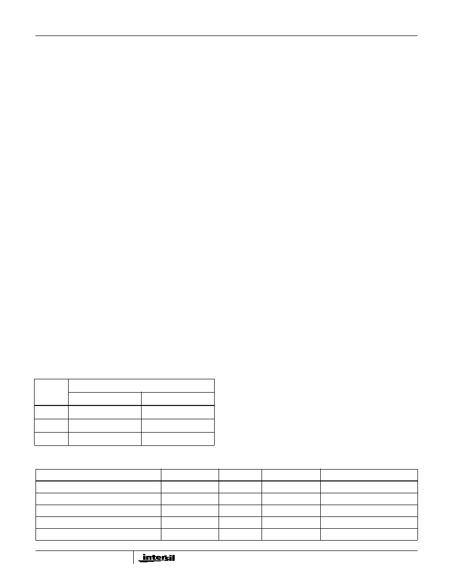
GAIN
(ACL)
CONNECTIONS
+INPUT
-INPUT
-1
50
to GND
Input
+1
Input
NC (Floating)
+2
Input
GND
TABLE 1. UNITY GAIN PERFORMANCE FOR VARIOUS IMPLEMENTATIONS
APPROACH
PEAKING (dB)
BW (MHz)
SR (V/
s)
±0.1dB GAIN FLATNESS (MHz)
Remove -IN Pin
5.0
550
1300
18
+RS = 620
1.0
230
1000
25
+RS = 620 and Remove -IN Pin
0.7
225
1000
28
Short +IN to -IN (e.g., Pins 2 and 3)
0.1
370
500
170
100pF Capacitor Between +IN and -IN
0.3
380
550
130
HS-1412RH
相关PDF资料 |
PDF描述 |
|---|---|
| 5962F9683401VCX | QUAD BUFFER AMPLIFIER, CDIP14 |
| 5962L9950401VCA | QUAD OP-AMP, 7000 uV OFFSET-MAX, 1 MHz BAND WIDTH, CDIP14 |
| 5962L9950401VDA | QUAD OP-AMP, 7000 uV OFFSET-MAX, 1 MHz BAND WIDTH, CDFP14 |
| 5962L9950401VZA | QUAD OP-AMP, 7000 uV OFFSET-MAX, 1 MHz BAND WIDTH, CDSO14 |
| 5962P0052401QGA | COMPARATOR, 4000 uV OFFSET-MAX, 200 ns RESPONSE TIME, MBCY8 |
相关代理商/技术参数 |
参数描述 |
|---|---|
| 5962F9861301VCC | 制造商:Intersil Corporation 功能描述: |
| 5962F9861301VHA | 制造商:Intersil Corporation 功能描述:- Bulk |
| 5962F9861301VXC | 制造商:Intersil Corporation 功能描述: |
| 5962F9865102QYA | 制造商:STMicroelectronics 功能描述:EIA-644LINE DRIVERQUADFLAT16, SOLDER DIP - Bulk |
| 5962F9865102QYC | 制造商:STMicroelectronics 功能描述:EIA-644LINE DRIVERQUADFLAT16, GOLD - Bulk |
发布紧急采购,3分钟左右您将得到回复。