- 您现在的位置:买卖IC网 > PDF目录56746 > 5962R9675501VJX (INTERSIL CORP) PARALLEL, WORD INPUT LOADING, 0.35 us SETTLING TIME, 12-BIT DAC, CDIP24 PDF资料下载
参数资料
| 型号: | 5962R9675501VJX |
| 厂商: | INTERSIL CORP |
| 元件分类: | DAC |
| 英文描述: | PARALLEL, WORD INPUT LOADING, 0.35 us SETTLING TIME, 12-BIT DAC, CDIP24 |
| 封装: | SIDE BRAZED, DIP-24 |
| 文件页数: | 3/7页 |
| 文件大小: | 125K |
| 代理商: | 5962R9675501VJX |
3
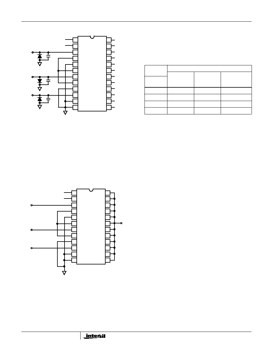
Burn-In Bias Circuit
NOTES:
D1 = D2 = D3 = IN4002 or Equivalent
F0 to F11:
VIH = 5.0V
±0.5V
VIL = 0.0V
±0.5V
F0 = 100kHz
±10% (50% Duty Cycle)
F1 = F0/2
F7 = F0/128
F2 = F0/4
F8 = F0/256
F3 = F0/8
F9 = F0/512
F4 = F0/16
F10 = F0/1024
F5 = F0/32
F11 = F0/2048
F6 = F0/64
Radiation Bias Circuit
NOTE: Power Supply Levels are 0.5V
Denitions of Specications
Digital Inputs
The HS-565ARH accepts digital input codes in binary format
and may be user connected for any one of three binary
codes. Straight binary, Two’s Complement (see note below),
or Offset Binary, (See Operating Instructions).
Accuracy
Nonlinearity - Nonlinearity of a D/A converter is an
important measure of its accuracy. It describes the deviation
from an ideal straight line transfer curve drawn between zero
(all bits OFF) and full scale (all bits ON).
Differential Nonlinearity - For a D/A converter, it is the
difference between the actual output voltage change and the
ideal (1 LSB) voltage change for a one bit change in code. A
Differential Nonlinearity of
±1 LSB or less guarantees
monotonicity; i.e., the output always increases and never
decreases for an increasing input.
Settling Time
Settling time is the time required for the output to settle to
within the specied error band for any input code transition.
It is usually specied for a full scale or major carry transition,
settling to within 0.50 LSB of nal value.
Drift
Gain Drift - The change in full scale analog output over the
specified temperature range expressed in parts per million of
full scale range per oC (ppm of FSR/oC). Gain error is
measured with respect to 25oC at high (TH) and low (TL)
temperatures. Gain drift is calculated for both high (TH -
25oC) and low ranges (25oC - TL) by dividing the gain error by
the respective change in temperature. The specification is the
larger of the two representing worst case drift.
Offset Drift - The change in analog output with all bits OFF
over the specied temperature range expressed in parts per
million of full scale range per oC (ppm of FSR/oC). Offset
error is measured with respect to 25oC at high (TH) and low
(TL) temperatures. Offset drift is calculated for both high (TH
- 25oC) and low (25oC - TL) ranges by dividing the offset
error by the respective change in temperature. The
C3
D3
+10V
1
4
5
8
9
10
11
12
16
17
18
19
20
21
22
23
24
15
14
13
2
3
6
7
NC
C1
D1
+15V
C2
D2
-15V
F0
F1
F2
F3
F4
F5
F6
F7
F8
F9
F10
F11
NC
VCC
REF GND
REF OUT
REF IN
-VEE
BIP OFF
OUT
10V SPAN
20V SPAN
PWR GND
BIT 1
BIT 2
BIT 3
BIT 4
BIT 5
BIT 6
BIT 7
BIT 8
BIT 9
BIT 10
BIT 11
BIT 12
+15V
1
4
5
8
9
10
11
12
16
17
18
19
20
21
22
23
24
15
14
13
2
3
6
7
NC
VCC
REF GND
REF OUT
REF IN
-VEE
BIP OFF
OUT
10V SPAN
20V SPAN
PWR GND
BIT 1
BIT 2
BIT 3
BIT 4
BIT 5
BIT 6
BIT 7
BIT 8
BIT 9
BIT 10
BIT 11
BIT 12
-15V
+10V
+5V
DIGITAL
INPUT
ANALOG OUTPUT
STRAIGHT
BINARY
OFFSET
BINARY
(NOTE)
TWO’S
COMPLEMENT
MSB...LSB
000 ... 000
Zero
-FS (Full Scale)
Zero
100 ... 000
0.50 FS
Zero
-FS
111 ... 111
+FS - 1LSB
Zero - 1LSB
011 ... 111
0.50 FS - 1LSB
Zero - 1LSB
+FS - 1LSB
NOTE: Invert MSB with external inverter to obtain Two’s
Complement Coding
HS-565ARH
相关PDF资料 |
PDF描述 |
|---|---|
| 5962R9675501VJX | PARALLEL, WORD INPUT LOADING, 0.35 us SETTLING TIME, 12-BIT DAC, CDIP24 |
| 5962R9675501VXX | PARALLEL, WORD INPUT LOADING, 0.35 us SETTLING TIME, 12-BIT DAC, CQFP24 |
| 59643-1 | BAND PASS FILTER |
| 59643-2 | BAND PASS FILTER |
| F4319 | BAND PASS FILTER |
相关代理商/技术参数 |
参数描述 |
|---|---|
| 5962R9679801VCA | 功能描述:校验器 IC RoHS:否 制造商:STMicroelectronics 产品: 比较器类型: 通道数量: 输出类型:Push-Pull 电源电压-最大:5.5 V 电源电压-最小:1.1 V 补偿电压(最大值):6 mV 电源电流(最大值):1350 nA 响应时间: 最大工作温度:+ 125 C 安装风格:SMD/SMT 封装 / 箱体:SC-70-5 封装:Reel |
| 5962R9679801VHA | 功能描述:校验器 IC RoHS:否 制造商:STMicroelectronics 产品: 比较器类型: 通道数量: 输出类型:Push-Pull 电源电压-最大:5.5 V 电源电压-最小:1.1 V 补偿电压(最大值):6 mV 电源电流(最大值):1350 nA 响应时间: 最大工作温度:+ 125 C 安装风格:SMD/SMT 封装 / 箱体:SC-70-5 封装:Reel |
| 5962R9679801VIA | 功能描述:校验器 IC RoHS:否 制造商:STMicroelectronics 产品: 比较器类型: 通道数量: 输出类型:Push-Pull 电源电压-最大:5.5 V 电源电压-最小:1.1 V 补偿电压(最大值):6 mV 电源电流(最大值):1350 nA 响应时间: 最大工作温度:+ 125 C 安装风格:SMD/SMT 封装 / 箱体:SC-70-5 封装:Reel |
| 5962R9679801VXA | 功能描述:校验器 IC RoHS:否 制造商:STMicroelectronics 产品: 比较器类型: 通道数量: 输出类型:Push-Pull 电源电压-最大:5.5 V 电源电压-最小:1.1 V 补偿电压(最大值):6 mV 电源电流(最大值):1350 nA 响应时间: 最大工作温度:+ 125 C 安装风格:SMD/SMT 封装 / 箱体:SC-70-5 封装:Reel |
| 5962R9679802VCA | 制造商:Texas Instruments 功能描述:5962R9679802VCA HIGH SPEED DUAL COMPARAT - Rail/Tube |
发布紧急采购,3分钟左右您将得到回复。