- 您现在的位置:买卖IC网 > PDF目录223059 > 8400110EKILF (INTEGRATED DEVICE TECHNOLOGY INC) OTHER CLOCK GENERATOR, QCC32 PDF资料下载
参数资料
| 型号: | 8400110EKILF |
| 厂商: | INTEGRATED DEVICE TECHNOLOGY INC |
| 元件分类: | XO, clock |
| 英文描述: | OTHER CLOCK GENERATOR, QCC32 |
| 封装: | 5 X 5 MM, 0.925 MM HEIGHT, ROHS COMPLIANT, MO-220VHHD-2, VFQFN-32 |
| 文件页数: | 14/14页 |
| 文件大小: | 699K |
| 代理商: | 8400110EKILF |
ICS8400110I Data Sheet
LOW JITTER, TELCOM RATE-CONVERSION PLL
ICS8400110EKI REVISION A NOVEMBER 9, 2009
9
2009 Integrated Device Technology, Inc.
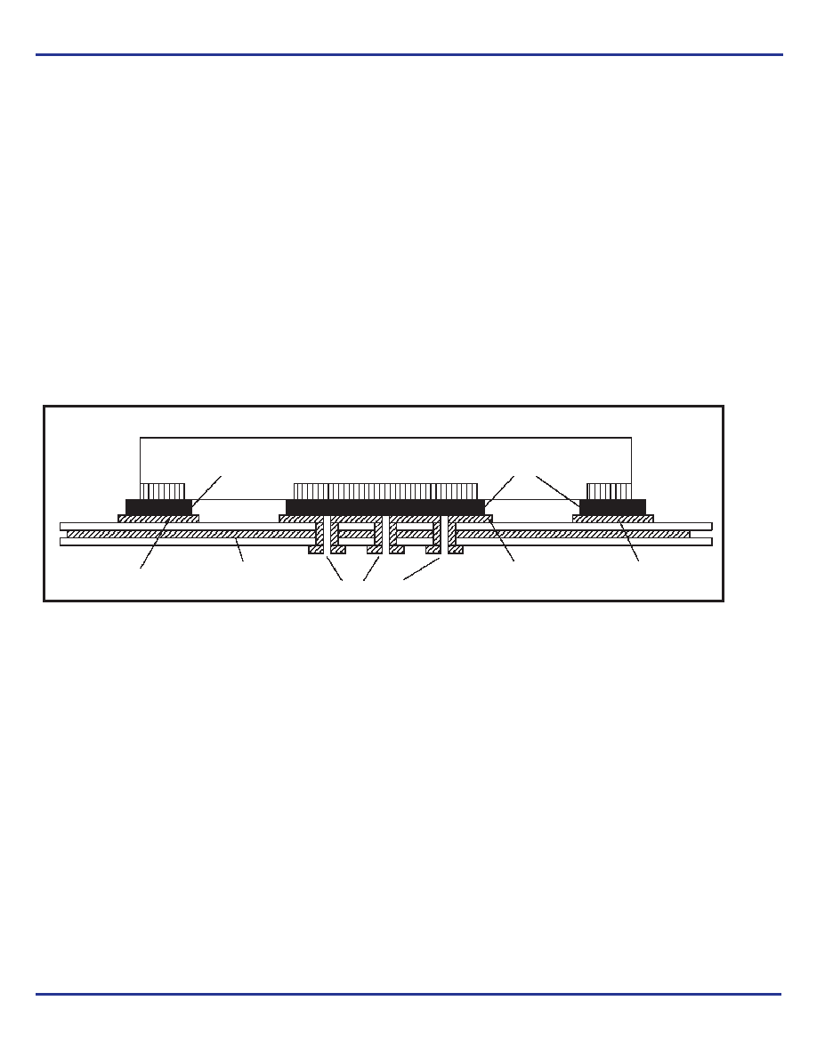
VFQFN EPAD Thermal Release Path
In order to maximize both the removal of heat from the package and
the electrical performance, a land pattern must be incorporated on
the Printed Circuit Board (PCB) within the footprint of the package
corresponding to the exposed metal pad or exposed heat slug on the
package, as shown in Figure 4. The solderable area on the PCB, as
defined by the solder mask, should be at least the same size/shape
as the exposed pad/slug area on the package to maximize the
thermal/electrical performance. Sufficient clearance should be
designed on the PCB between the outer edges of the land pattern
and the inner edges of pad pattern for the leads to avoid any shorts.
While the land pattern on the PCB provides a means of heat transfer
and electrical grounding from the package to the board through a
solder joint, thermal vias are necessary to effectively conduct from
the surface of the PCB to the ground plane(s). The land pattern must
be connected to ground through these vias. The vias act as “heat
pipes”. The number of vias (i.e. “heat pipes”) are application specific
and dependent upon the package power dissipation as well as
electrical conductivity requirements. Thus, thermal and electrical
analysis and/or testing are recommended to determine the minimum
number needed. Maximum thermal and electrical performance is
achieved when an array of vias is incorporated in the land pattern. It
is recommended to use as many vias connected to ground as
possible. It is also recommended that the via diameter should be 12
to 13mils (0.30 to 0.33mm) with 1oz copper via barrel plating. This is
desirable to avoid any solder wicking inside the via during the
soldering process which may result in voids in solder between the
exposed pad/slug and the thermal land. Precautions should be taken
to eliminate any solder voids between the exposed heat slug and the
land pattern. Note: These recommendations are to be used as a
guideline only. For further information, please refer to the Application
Note on the Surface Mount Assembly of Amkor’s Thermally/
Electrically Enhance Leadframe Base Package, Amkor Technology.
Figure 4. P.C. Assembly for Exposed Pad Thermal Release Path – Side View (drawing not to scale)
SOLDER
PIN
EXPOSED HEAT SLUG
PIN PAD
GROUND PLANE
LAND PATTERN
(GROUND PAD)
THERMAL VIA
相关PDF资料 |
PDF描述 |
|---|---|
| 84013036 | INTERCONNECTION DEVICE |
| 8403612LX | 2K X 8 STANDARD SRAM, 70 ns, CDIP24 |
| 841 | FEMALE, D SUBMINIATURE CONNECTOR, IDC, RECEPTACLE |
| 842-864-0499-001 | 4 CONTACT(S), MALE, POWER CONNECTOR, SURFACE MOUNT, PLUG |
| 843002AKI-40LF | 175 MHz, OTHER CLOCK GENERATOR, QCC32 |
相关代理商/技术参数 |
参数描述 |
|---|---|
| 840011AG | 制造商:Integrated Device Technology Inc 功能描述:840011AG - Rail/Tube |
| 840011AGI | 制造商:Integrated Device Technology Inc 功能描述:840011AGI - Rail/Tube |
| 840011AGIT | 制造商:Integrated Device Technology Inc 功能描述:PLL CLOCK GEN SGL 8TSSOP - Tape and Reel |
| 840011AGLN | 功能描述:时钟发生器及支持产品 RoHS:否 制造商:Silicon Labs 类型:Clock Generators 最大输入频率:14.318 MHz 最大输出频率:166 MHz 输出端数量:16 占空比 - 最大:55 % 工作电源电压:3.3 V 工作电源电流:1 mA 最大工作温度:+ 85 C 安装风格:SMD/SMT 封装 / 箱体:QFN-56 |
| 840011AGLNT | 制造商:Integrated Device Technology Inc 功能描述:PLL Clock Generator Single 8-Pin TSSOP T/R 制造商:Integrated Device Technology Inc 功能描述:8 TSSOP (LEAD-FREE) - Tape and Reel |
发布紧急采购,3分钟左右您将得到回复。