- 您现在的位置:买卖IC网 > PDF目录24830 > 935270667118 (NXP SEMICONDUCTORS) PLL BASED CLOCK DRIVER, 10 TRUE OUTPUT(S), 0 INVERTED OUTPUT(S), PDSO48 PDF资料下载
参数资料
| 型号: | 935270667118 |
| 厂商: | NXP SEMICONDUCTORS |
| 元件分类: | 时钟及定时 |
| 英文描述: | PLL BASED CLOCK DRIVER, 10 TRUE OUTPUT(S), 0 INVERTED OUTPUT(S), PDSO48 |
| 封装: | 4.40 MM, 0.40 MM PITCH, PLASTIC, MO-153, SOT-480-1, TVSOP-48 |
| 文件页数: | 11/15页 |
| 文件大小: | 113K |
| 代理商: | 935270667118 |
Philips Semiconductors
Product data
PCKV857
70–190 MHz differential 1:10 clock driver
2002 Sep 13
5
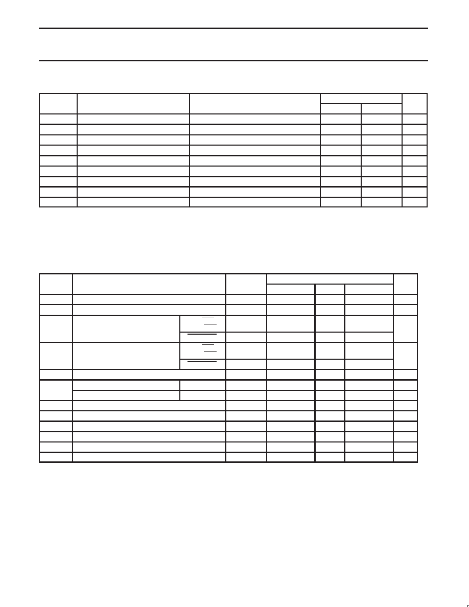
ABSOLUTE MAXIMUM RATINGS1
SYMBOL
PARAMETER
CONDITION
LIMITS
UNIT
SYMBOL
PARAMETER
CONDITION
MIN
MAX
UNIT
VDDQ
Supply voltage range
0.5
3.6
V
AVDD
Supply voltage range
0.5
3.6
V
VI
Input voltage range
see Notes 2 and 3
–0.5
VDDQ + 0.5
V
VO
Output voltage range
see Notes 2 and 3
–0.5
VDDQ + 0.5
V
IIK
Input clamp current
VI < 0 or VI >VDDQ
—
±50
mA
IOK
Output clamp current
VO < 0 or VO >VDDQ
—
±50
mA
IO
Continuous output current
VO = 0 to VDDQ
—
±50
mA
Continuous current to GND or VDDQ
—
±100
mA
Tstg
Storage temperature range
–65
+150
°C
NOTES:
1. Stresses beyond those listed under “absolute maximum ratings” may cause permanent damage to the device. These are stress ratings
only, and functional operation of the device at these or any other conditions beyond those indicated under “recommended operating
conditions” is not implied. Exposure to absolute-maximum-rated conditions for extended periods may affect device reliability.
2. The input and output negative voltage ratings may be exceeded if the input and output clamp-current ratings are observed.
3. This value is limited to 3.6 V maximum.
RECOMMENDED OPERATING CONDITIONS1
SYMBOL
PARAMETER
CONDITION
LIMITS
UNIT
SYMBOL
PARAMETER
CONDITION
MIN
TYP
MAX
UNIT
VDDQ
Supply voltage range
2.3
—
2.7
V
AVDD
Supply voltage range
2.2
—
2.7
V
VIL
Low level input voltage
CLK, CLK,
FBIN, FBIN
—
VDDQ/2 0.18
V
IL
g
PWRDWN
0.3
—
0.7
VIH
High level input voltage
CLK, CLK,
FBIN, FBIN
VDDQ/2 + 0.18
—
V
IH
gg
PWRDWN
1.7
—
VDDQ + 0.3
DC input signal voltage
Note 2
0.3
—
VDDQ
V
DC differential input signal voltage
CLK, FBIN
Note 3
0.36
—
VDDQ + 0.6
V
VID
AC differential input signal voltage
CLK, FBIN
Note 3
0.7
—
VDDQ + 0.6
V
VOX
Output differential cross-voltage
Note 4
VDDQ/2 0.2
VDDQ/2
VDDQ/2 + 0.2
V
VIX
Input differential cross-voltage
Note 4
VDDQ/2 0.2
—
VDDQ/2 + 0.2
V
IOH
High-level output current
—
12
mA
IOL
Low-level output current
—
12
mA
SR
Input slew rate
1
—
4
V/ns
Tamb
Operating free-air temperature
0
—
70
°C
NOTES:
1. Unused inputs must be held high or low to prevent them from floating.
2. DC input signal voltage specifies the allowable DC execution of differential input.
3. Differential input signal voltage specifies the differential voltage |VTR – VCP| required for switching, where VTR is the true input level and
VCP is the complementary input level.
4. Differential cross-point voltage is expected to track variations of VCC and is the voltage at which the differential signals must be crossing.
相关PDF资料 |
PDF描述 |
|---|---|
| 935269132118 | PLL BASED CLOCK DRIVER, 10 TRUE OUTPUT(S), 0 INVERTED OUTPUT(S), PDSO48 |
| 935269202112 | 8 I/O, PIA-GENERAL PURPOSE, PDSO16 |
| 935269193112 | 8 I/O, PIA-GENERAL PURPOSE, PDSO16 |
| 935269192112 | 8 I/O, PIA-GENERAL PURPOSE, PDSO16 |
| 935269192118 | 8 I/O, PIA-GENERAL PURPOSE, PDSO16 |
相关代理商/技术参数 |
参数描述 |
|---|---|
| 935270713557 | 制造商:NXP Semiconductors 功能描述:SUB ONLY IC CHP |
| 935270792551 | 制造商:NXP Semiconductors 功能描述:IC BUFF DVR TRI-ST 16BIT 56VFBGA |
| 935270792557 | 制造商:NXP Semiconductors 功能描述:IC BUFF DVR TRI-ST 16BIT 56VFBGA |
| 935270793551 | 制造商:NXP Semiconductors 功能描述:IC BUS TRCVR 3-ST 16BIT 56VFBGA |
| 935270793557 | 制造商:NXP Semiconductors 功能描述:IC BUS TRCVR 3-ST 16BIT 56VFBGA |
发布紧急采购,3分钟左右您将得到回复。