- 您现在的位置:买卖IC网 > PDF目录24830 > 935270667118 (NXP SEMICONDUCTORS) PLL BASED CLOCK DRIVER, 10 TRUE OUTPUT(S), 0 INVERTED OUTPUT(S), PDSO48 PDF资料下载
参数资料
| 型号: | 935270667118 |
| 厂商: | NXP SEMICONDUCTORS |
| 元件分类: | 时钟及定时 |
| 英文描述: | PLL BASED CLOCK DRIVER, 10 TRUE OUTPUT(S), 0 INVERTED OUTPUT(S), PDSO48 |
| 封装: | 4.40 MM, 0.40 MM PITCH, PLASTIC, MO-153, SOT-480-1, TVSOP-48 |
| 文件页数: | 8/15页 |
| 文件大小: | 113K |
| 代理商: | 935270667118 |
Philips Semiconductors
Product data
PCKV857
70–190 MHz differential 1:10 clock driver
2
2002 Sep 13
FEATURES
ESD classification testing is done to JEDEC Standard JESD22.
Protection exceeds 2000 V to HBM per method A114.
Latch-up testing is done to JEDEC Standard JESD78 which
exceeds 100 mA
Optimized for clock distribution in DDR (Double Data Rate)
SDRAM applications as per JEDEC specifications
1-to-10 differential clock distribution
Very low skew (< 100 ps) and jitter (< 100 ps)
Operation from 2.2 V to 2.7 V AV
DD and 2.3 V to 2.7 V VDD
SSTL_2 interface clock inputs and outputs
CMOS control signal input
Test mode enables buffers while disabling PLL
Low current power-down mode
Tolerant of Spread Spectrum input clock
Full DDR solution provided when used with SSTL16877 or
SSTV16857
Designed for DDR 200 and 266 DIMM applications
Available in TSSOP-48, TVSOP-48, and VFBGA56
(8 no connects) packages
DESCRIPTION
The PCKV857 is a high-performance, low-skew, low-jitter zero delay
buffer designed for 2.5 V VDD and 2.5 V AVDD operation and
differential data input and output levels.
The PCKV857 is a zero delay buffer that distributes a differential
clock input pair (CLK, CLK) to ten differential pairs of clock outputs
(Y[0:9], Y[0:9]) and one differential pair feedback clock outputs
(FBOUT, FBOUT) . The clock outputs are controlled by the clock
inputs (CLK, CLK), the feedback clocks (FBIN, FBIN), and the analog
power input (AVDD). When PWRDWN is high, the outputs switch in
phase and frequency with CLK. When PWRDWN is low, all outputs
are disabled to high impedance state (3-State), and the PLL is shut
down (low power mode). The device also enters the low power
mode when the input frequency falls below 20 MHz. An input
frequency detection circuit will detect the low frequency condition
and after applying a > 20 MHz input signal, the detection circuit
turns on the PLL again and enables the outputs.
When AVDD is grounded, the PLL is turned off and bypassed for test
purposes. The PCKV857 is also able to track spread spectrum
clocking for reduced EMI.
The PCKV857 is characterized for operation from 0 to +70
°C.
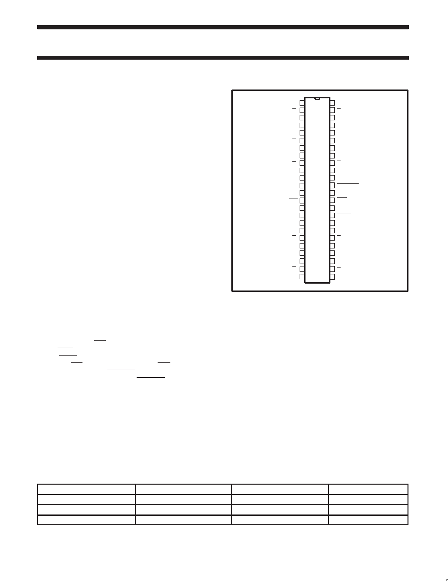
PIN CONFIGURATION
1
2
3
4
5
6
7
8
9
10
11
12
13
14
15
16
17
18
19
20
25
26
27
28
29
30
31
32
33
34
35
36
37
38
39
40
21
22
23
24
41
42
43
44
45
46
47
48
GND
Y0
VDDQ
Y1
GND
Y2
GND
Y2
VDDQ
CLK
VDDQ
AVDD
AGND
GND
Y3
VDDQ
Y4
GND
Y5
VDDQ
Y6
GND
Y7
VDDQ
PWRDWN
FBIN
VDDQ
FBOUT
GND
Y8
VDDQ
Y9
SW00691
GND
ORDERING INFORMATION
PACKAGES
TEMPERATURE RANGE
ORDER CODE
DRAWING NUMBER
48-Pin Plastic TSSOP
0 to +70
°C
PCKV857DGG
SOT362-1
48-Pin Plastic TSSOP (TVSOP)
0 to +70
°C
PCKV857DGV
SOT480-1
56-ball Plastic VFBGA1
0 to +70
°C
PCKV857EV
SOT702-1
NOTE:
1. 48 balls are connected, 8 balls are no-connects.
相关PDF资料 |
PDF描述 |
|---|---|
| 935269132118 | PLL BASED CLOCK DRIVER, 10 TRUE OUTPUT(S), 0 INVERTED OUTPUT(S), PDSO48 |
| 935269202112 | 8 I/O, PIA-GENERAL PURPOSE, PDSO16 |
| 935269193112 | 8 I/O, PIA-GENERAL PURPOSE, PDSO16 |
| 935269192112 | 8 I/O, PIA-GENERAL PURPOSE, PDSO16 |
| 935269192118 | 8 I/O, PIA-GENERAL PURPOSE, PDSO16 |
相关代理商/技术参数 |
参数描述 |
|---|---|
| 935270713557 | 制造商:NXP Semiconductors 功能描述:SUB ONLY IC CHP |
| 935270792551 | 制造商:NXP Semiconductors 功能描述:IC BUFF DVR TRI-ST 16BIT 56VFBGA |
| 935270792557 | 制造商:NXP Semiconductors 功能描述:IC BUFF DVR TRI-ST 16BIT 56VFBGA |
| 935270793551 | 制造商:NXP Semiconductors 功能描述:IC BUS TRCVR 3-ST 16BIT 56VFBGA |
| 935270793557 | 制造商:NXP Semiconductors 功能描述:IC BUS TRCVR 3-ST 16BIT 56VFBGA |
发布紧急采购,3分钟左右您将得到回复。