- 您现在的位置:买卖IC网 > PDF目录24830 > 935270667118 (NXP SEMICONDUCTORS) PLL BASED CLOCK DRIVER, 10 TRUE OUTPUT(S), 0 INVERTED OUTPUT(S), PDSO48 PDF资料下载
参数资料
| 型号: | 935270667118 |
| 厂商: | NXP SEMICONDUCTORS |
| 元件分类: | 时钟及定时 |
| 英文描述: | PLL BASED CLOCK DRIVER, 10 TRUE OUTPUT(S), 0 INVERTED OUTPUT(S), PDSO48 |
| 封装: | 4.40 MM, 0.40 MM PITCH, PLASTIC, MO-153, SOT-480-1, TVSOP-48 |
| 文件页数: | 13/15页 |
| 文件大小: | 113K |
| 代理商: | 935270667118 |
Philips Semiconductors
Product data
PCKV857
70–190 MHz differential 1:10 clock driver
2002 Sep 13
7
AC CHARACTERISTICS
GND = 0 V; tr = tf ≤ 2.5 ns; CL = 50 pF; RL = 1 k
SYMBOL
PARAMETER
WAVEFORM
CONDITION
LIMITS
UNIT
SYMBOL
PARAMETER
WAVEFORM
CONDITION
MIN
TYP
MAX
UNIT
t(O)
Static phase offset
Figure 1
–150
0
150
ps
tSK(O)
Output clock skew
Figure 2
—
75
ps
tSLR(O)
Output clock skew rate
Figure 3
1
—
2
V/ns
tJIT(PER)
Jitter (period)
Figure 4
fO = 67 MHz to 200 MHz
–75
—
75
ps
tJIT(CC)
Jitter (cycle-to-cycle)
Figure 5
fO = 67 MHz to 200 MHz
–75
—
75
ps
tJIT(HPER)
Half-period jitter
Figure 6
–100
—
100
ps
tPLH1
Low to high level
propagation delay
Test mode/CLK to any
output
—
3.7
—
ns
tPHL1
High to low level
propagation delay
Test mode/CLK to any
output
—
3.7
—
ns
NOTE:
1. Refers to transition of noninverting output.
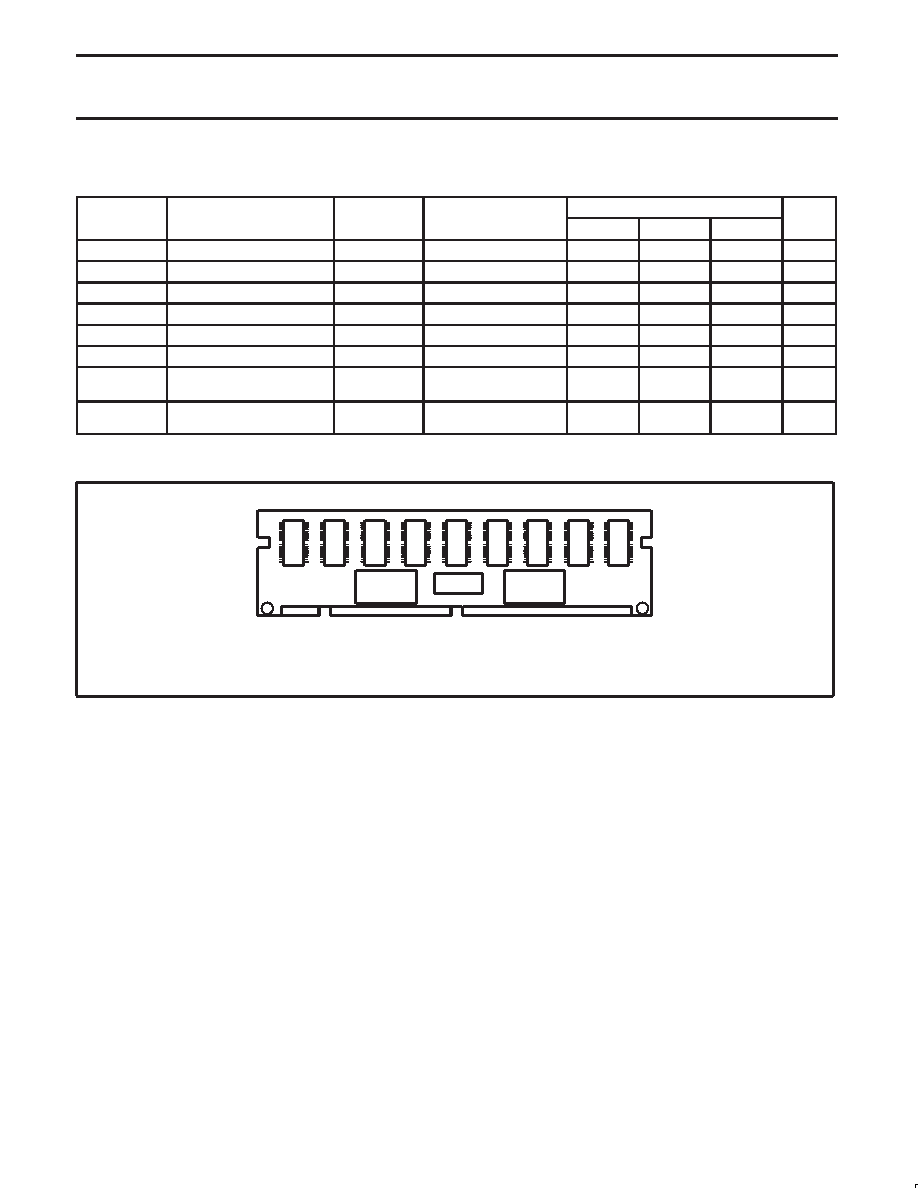
The PLL clock distribution device and SSTL registered drivers reduce
signal loads on the memory controller and prevent timing delays and
waveform distortions that would cause unreliable operation
SW00688
SDRAM
SSTL16877
or
SSTV16857
PCKV857
FRONT SIDE
SSTL16877
or
SSTV16857
相关PDF资料 |
PDF描述 |
|---|---|
| 935269132118 | PLL BASED CLOCK DRIVER, 10 TRUE OUTPUT(S), 0 INVERTED OUTPUT(S), PDSO48 |
| 935269202112 | 8 I/O, PIA-GENERAL PURPOSE, PDSO16 |
| 935269193112 | 8 I/O, PIA-GENERAL PURPOSE, PDSO16 |
| 935269192112 | 8 I/O, PIA-GENERAL PURPOSE, PDSO16 |
| 935269192118 | 8 I/O, PIA-GENERAL PURPOSE, PDSO16 |
相关代理商/技术参数 |
参数描述 |
|---|---|
| 935270713557 | 制造商:NXP Semiconductors 功能描述:SUB ONLY IC CHP |
| 935270792551 | 制造商:NXP Semiconductors 功能描述:IC BUFF DVR TRI-ST 16BIT 56VFBGA |
| 935270792557 | 制造商:NXP Semiconductors 功能描述:IC BUFF DVR TRI-ST 16BIT 56VFBGA |
| 935270793551 | 制造商:NXP Semiconductors 功能描述:IC BUS TRCVR 3-ST 16BIT 56VFBGA |
| 935270793557 | 制造商:NXP Semiconductors 功能描述:IC BUS TRCVR 3-ST 16BIT 56VFBGA |
发布紧急采购,3分钟左右您将得到回复。