- 您现在的位置:买卖IC网 > PDF目录24864 > 950908BGLF-T (INTEGRATED DEVICE TECHNOLOGY INC) 200.4 MHz, PROC SPECIFIC CLOCK GENERATOR, PDSO56 PDF资料下载
参数资料
| 型号: | 950908BGLF-T |
| 厂商: | INTEGRATED DEVICE TECHNOLOGY INC |
| 元件分类: | 时钟产生/分配 |
| 英文描述: | 200.4 MHz, PROC SPECIFIC CLOCK GENERATOR, PDSO56 |
| 封装: | 0.240 INCH, 0.020 INCH PITCH, GREEN, MO-153, TSSOP-56 |
| 文件页数: | 18/24页 |
| 文件大小: | 305K |
| 代理商: | 950908BGLF-T |
3
Integrated
Circuit
Systems, Inc.
ICS950908
Preliminary Product Preview
0653A—07/26/04
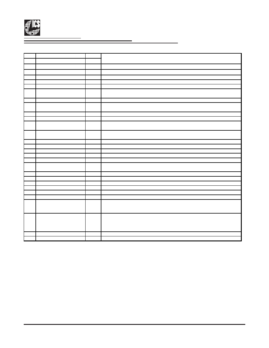
Pin Description
PIN
#
NAME
TYPE
1
*FS0/REF0
I/O
Frequency select latch input pin / 14.318 MHz reference clock.
2
GND
PWR
Ground pin.
3
X1
IN
Crystal input, Nominally 14.318MHz.
4
X2
OUT
Crystal output, Nominally 14.318MHz
5
VDDAGP
PWR
Power supply for AGP clocks, nominal 3.3V
6
*MODE/AGPCLK0
I/O
Function select latch input pin, 1=Desktop Mode, 0=Mobile Mode / AGP clock output.
7
*SEL_408/K7/AGPCLK1
I/O
CPU output type select latch input pin 0= K7, 1= CK408 / AGP clock output.
8
*(PCI_STOP#)AGPCLK2
I/O
Stops all PCICLKs besides the PCICLK_F clocks at logic 0 level, when input low. This
input is activated by the MODE selection pin / AGP clock output.
9
GNDAGP
PWR
Ground pin for the AGP outputs
10
**FS1/PCICLK_F
I/O
Frequency select latch input pin / 3.3V PCI free running clock output.
11
**SEL_SDR/DDR#/PCICLK1
I/O
Memory type select latch input pin 0= DDR, 1= PC133 SDRAM / 3.3V PCI clock output.
12
*MULTSEL/PCICLK2
I/O
3.3V LVTTL input for selection the current multiplier for CPU outputs / 3.3V PCI clock
output.
13
GNDPCI
PWR
Ground pin for the PCI outputs
14
PCICLK3
OUT
PCI clock output.
15
PCICLK4
OUT
PCI clock output.
16
VDDPCI
PWR
Power supply for PCI clocks, nominal 3.3V
17
PCICLK5
OUT
PCI clock output.
18
*(CLK_STOP#)/PCICLK6
I/O
Stops all CPU, DDR/SDRAM and FB_OUT clocks at logic 0 level, when input low. This
input is activated by the MODE selection pin / PCI clock output.
19
GND48
PWR
Ground pin for the 48MHz outputs
20
*FS3/48MHz
I/O
Frequency select latch input pin / Fixed 48MHz clock output. 3.3V
21
*FS2/24_48MHz
I/O
Frequency select latch input pin / Fixed 24 or 48MHz clock output. 3.3V.
22
AVDD48
PWR
Analog power for 48MHz outputs and fixed PLL core, nominal 3.3V
23
VDD
PWR
Power supply, nominal 3.3V
24
GND
PWR
Ground pin.
25
IREF
OUT
This pin establishes the reference current for the differential current-mode output pairs.
This pin requires a fixed precision resistor tied to ground in order to establish the
appropriate current. 475 ohms is the standard value.
26
*(PD#)RESET#
I/O
Asynchronous active low input pin used to power down the device into a low power
state. This input is activated by the MODE selection pin / Real time system reset
signal for frequency gear ratio change or watchdog timer timeout. This signal is active
low.
27
SCLK
IN
Clock pin of SMBus circuitry, 5V tolerant.
28
SDATA
I/O
Data pin for SMBus circuitry, 5V tolerant.
* Internal Pull-Up Resistor
** Internal Pull-Down Resistor
DESCRIPTION
~ This output has 2X drive strength
Pin description continued on next page.
相关PDF资料 |
PDF描述 |
|---|---|
| 950908BFLF | 200.4 MHz, PROC SPECIFIC CLOCK GENERATOR, PDSO56 |
| 950908BFLF-T | 200.4 MHz, PROC SPECIFIC CLOCK GENERATOR, PDSO56 |
| 08056C103KA74A | General Specifications |
| 950956 | MODULAR TERMINAL BLOCK |
| 950260 | MODULAR TERMINAL BLOCK |
相关代理商/技术参数 |
参数描述 |
|---|---|
| 9509130000 | 制造商:Weidmuller 功能描述:NPA6 NEXT PADLOCK HASP 制造商:Weidmuller 功能描述:NPA6,NEXT PADLOCK HASP |
| 9509136038 | 制造商:APEM 功能描述:Switch Accessories Led Red/yellow For 1E/1F/1Q/1R |
| 9509136105 | 制造商:APEM 功能描述:Navimec w caps w std legends, up arrow |
| 9509136118 | 制造商:Mec 功能描述:Bulk 制造商:MEC A/S 功能描述:SWITCH MODULE BLACK 制造商:MEC A/S 功能描述:SWITCH MODULE, BLACK 制造商:APEM 功能描述:5 SwitchMountModule w/OK+UP Arrow Legend 制造商:MEC A/S 功能描述:SWITCH, MODULE, 50mA, 24VDC; Contact Voltage DC Nom:24V; Contact Current Max:50mA; Actuator Style:-; Switch Terminals:Solder; Series:Navimec module ;RoHS Compliant: Yes 制造商:MEC 功能描述:Black 5 way PCB mounted switch |
| 9509136119 | 制造商:APEM 功能描述:Navimec w caps w std legends, up arrow/OK |
发布紧急采购,3分钟左右您将得到回复。