- 您现在的位置:买卖IC网 > PDF目录360630 > 95P04 (意法半导体) SERIAL ACCESS SPI BUS 4K 512 x 8 EEPROM PDF资料下载
参数资料
| 型号: | 95P04 |
| 厂商: | 意法半导体 |
| 英文描述: | SERIAL ACCESS SPI BUS 4K 512 x 8 EEPROM |
| 中文描述: | 串行访问SPI总线4K的512 × 8的EEPROM |
| 文件页数: | 7/16页 |
| 文件大小: | 151K |
| 代理商: | 95P04 |
C
Q
AI01072B
S
D
HOLD
tCLHX
tHXCH
tHXCH
tCLHX
tHHQX
tHLQZ
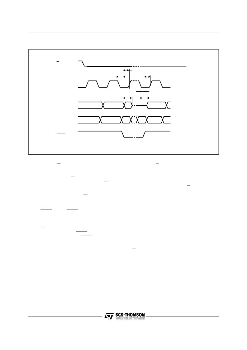
Figure 7. Hold Timing
Write Protect (W).
This pin is for hardware write
protect. When W is low, non-volatile writes to the
ST95P04 are disabled but any other operation
stays enabled. When W is high, all operations
including non-volatile writes are available. W going
low at any time before the last bit D0 of the data
stream will reset the write enable latch and prevent
programming. No action on W or on the write
enable latch can interrupt a write cycle which has
commenced.
Hold (HOLD).
The HOLD pin is used to pause
serial communications with a ST95P04 without
resetting the serial sequence. To take the Hold
condition into account, the product must be se-
lected (S = 0). Then the Hold state is validated by
a high to low transition on HOLD when C is low. To
resume the communications, HOLD is brought high
when C is low. During Hold condition D, Q, and C
are at a high impedance state.
When the ST95P04 is under Hold condition, it is
possible to deselect it. However, the serial commu-
nications will remain paused after a reselect, and
the chip will be reset.
OPERATIONS
All instructions, addresses and data are shifted in
and out of the chip MSB first. Data input (D) is
sampled on the first rising edge of clock (C) after
the chip select (S) goes low. Prior to any operation,
a one-byte instruction code must be entered in the
chip. This code is entered via the data input (D),
and latched on the rising edge of the clock input
(C). To enter an instruction code, the product must
have been previously selected (S = low). Table 7
shows the instruction set and format for device
operation. When an invalid instruction is sent (one
not contained in Table 7), the chip is automatically
deselected. For operations that read or write data
in the memory array, bit 3 of the instruction is the
MSB of the address, otherwise, it is a don’t care.
Write Enable (WREN) and Write Disable (WRDI)
The ST95P04 contains a write enable latch. This
latch must be set prior to every WRITE or WRSR
operation. The WREN instruction will set the latch
and the WRDI instruction will reset the latch. The
latch is reset under all the following conditions:
– W pin is low
– Power on
– WRDI instruction executed
– WRSR instruction executed
– WRITE instruction executed
As soon as the WREN or WRDI instruction is
received by the ST95P04, the circuit executes the
instruction and enters a wait mode until it is dese-
lected.
7/16
ST95P04
相关PDF资料 |
PDF描述 |
|---|---|
| 95PF120 | STANDARD RECOVERY DIODES GEN II DO5 |
| 95PF120W | STANDARD RECOVERY DIODES GEN II DO5 |
| 95PFR120W | STANDARD RECOVERY DIODES GEN II DO5 |
| 95PF40 | 400V 95A Std. Recovery Diode in a DO-5 package |
| 95PF80 | 800V 95A Std. Recovery Diode in a DO-5 package |
相关代理商/技术参数 |
参数描述 |
|---|---|
| 95PF120 | 制造商:Vishay Angstrohm 功能描述:Diode Switching 1.2KV 95A 2-Pin DO-5 制造商:Vishay Semiconductors 功能描述:STANDARD DIODE 95A 1.2KV DO-203AB |
| 95PF-120 | 制造商:TRSYS 制造商全称:Transys Electronics 功能描述:STANDARD RECOVERY DIODE |
| 95PF120W | 制造商:VISHAY 制造商全称:Vishay Siliconix 功能描述:Standard Recovery Diodes Generation 2 DO-5 (Stud Version), 95 A |
| 95PF140 | 制造商:VISHAY 制造商全称:Vishay Siliconix 功能描述:Standard Recovery Diodes Generation 2 DO-5 (Stud Version), 95 A |
| 95PF140_12 | 制造商:VISHAY 制造商全称:Vishay Siliconix 功能描述:Standard Recovery Diodes Generation 2 DO-5 (Stud Version), 95 A |
发布紧急采购,3分钟左右您将得到回复。