- 您现在的位置:买卖IC网 > PDF目录360630 > 95P04 (意法半导体) SERIAL ACCESS SPI BUS 4K 512 x 8 EEPROM PDF资料下载
参数资料
| 型号: | 95P04 |
| 厂商: | 意法半导体 |
| 英文描述: | SERIAL ACCESS SPI BUS 4K 512 x 8 EEPROM |
| 中文描述: | 串行访问SPI总线4K的512 × 8的EEPROM |
| 文件页数: | 8/16页 |
| 文件大小: | 151K |
| 代理商: | 95P04 |
Read Status Register (RDSR)
The RDSR instruction provides access to the status
register. The status register may be read at any
time, even during a non-volatile write. As soon as
the 8th bit of the status register is read out, the
ST95P04 enters a wait mode (data on D are not
decoded, Q is in Hi-Z) until it is deselected.
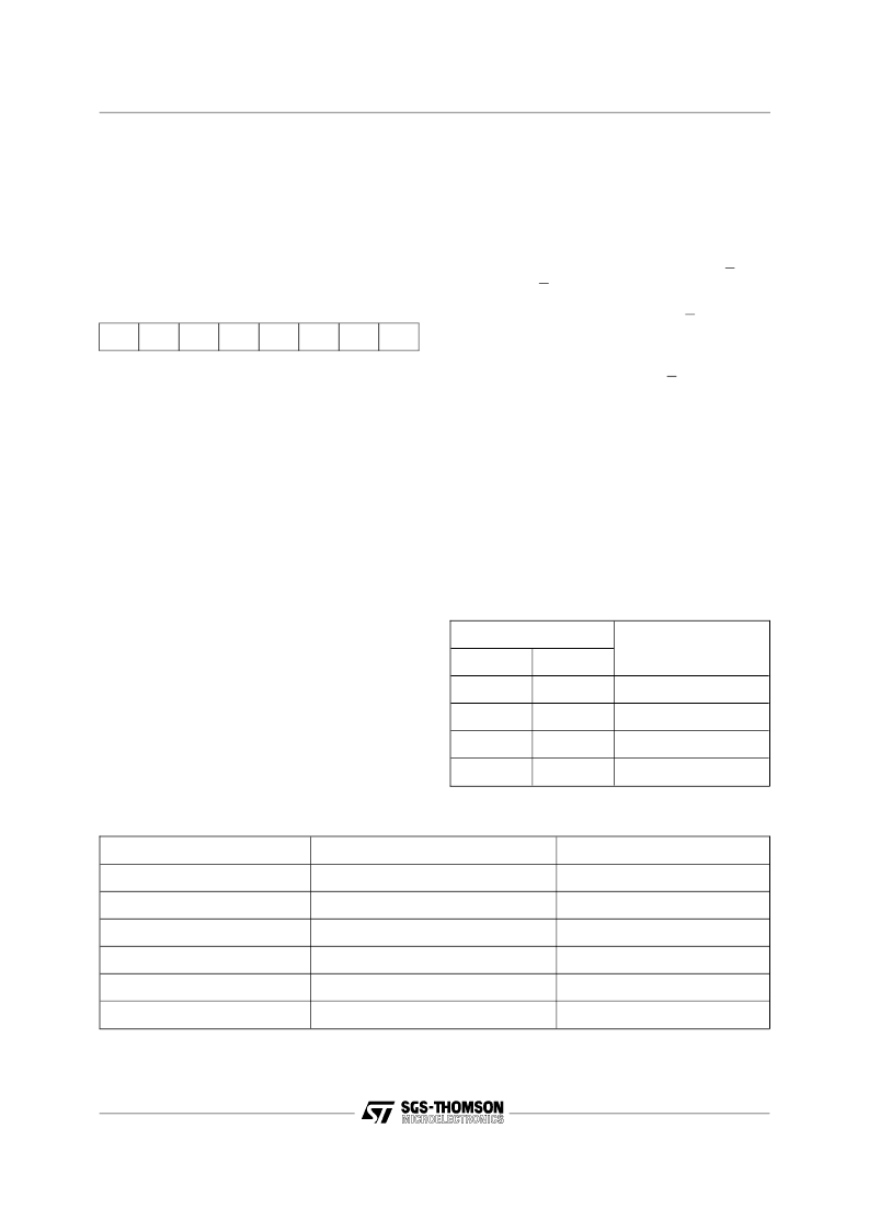
The status register format is as follows:
b7
b0
1
1
1
1
BP1
BP0
WEL
WIP
BP1, BP0: Read and Write bits
WEL, WIP: Read only bits.
During a non-volatile write to the memory array, all
bits BP1, BP0, WEL, WIP are valid and can be read.
During a non volatile write to the status register, the
only bits WEL and WIP are valid and can be read.
The values of BP1 and BP0 read at that time
correspond to the previous contents of the status
register.
The Write-In-Process (WIP) read only bit indicates
whether the ST95P04 is busy with a write opera-
tion. When set to a ’1’ a write is in progress, when
set to a ’0’ no write is in progress.
The Write Enable Latch (WEL) read only bit indi-
cates the status of the write enable latch. When set
to a ’1’ the latch is set, when set to a ’0’ the latch is
reset.
The Block Protect (BP0 and BP1) bits indicate the
extent of the protection employed. These bits are
set by the user issuing the WRSR instruction.
These bits are non-volatile.
Write Status Register (WRSR)
The WRSR instruction allows the user to select the
size of protected memory. The ST95P04 is divided
into four 1024 bit blocks. The user may read the
blocks but will be unable to write within the selected
blocks.
The blocks and respective WRSR control bits are
shown in Table 6.
When the WRSR instruction and the 8 bits of the
Status Register are latched-in, the internal write
cycle is then triggered by the rising edge of S. This
rising edge of S must appear after the 8th bit of the
Status Register content (it must not appear a 17th
clock pulse before the rising edge of S), otherwise
the internal write sequence is not performed.
Read Operation
The chip is first selected by putting S low. The serial
one byte read instruction is followed by a one byte
address (A7-A0), each bit being latched-in during
the rising edge of the clock (C). Bit 3 of the read
instruction contains address A8 (most significant
address bit). This bit is used to select the first or
second page of the device. Then, the data stored
in the memory at the selected address is shifted out
on the Q output pin; each bit being shifted out
during the falling edge of the clock (C). The data
stored in the memory at the next address can be
read in sequence by continuing to provide clock
Status Register Bits
Array Addresses
Protected
BP1
BP0
0
0
none
0
1
180h - 1FFh
1
0
100h - 1FFh
1
1
000h - 1FFh
Table 6. Array Addresses Protect
Instruction
Description
Instruction Format
WREN
Set Write Enable Latch
0000 X110
WRDI
Reset Write Enable Latch
0000 X100
RDSR
Read Status Register
0000 X101
WRSR
Write Status Register
0000 X001
READ
Read Data from Memory Array
0000 A011
WRITE
Write Data to Memory Array
0000 A010
Table 7. Instruction Set
Notes:
A = 1, Upper page selected
A = 0, Lower page selected
X = Don’t care
8/16
ST95P04
相关PDF资料 |
PDF描述 |
|---|---|
| 95PF120 | STANDARD RECOVERY DIODES GEN II DO5 |
| 95PF120W | STANDARD RECOVERY DIODES GEN II DO5 |
| 95PFR120W | STANDARD RECOVERY DIODES GEN II DO5 |
| 95PF40 | 400V 95A Std. Recovery Diode in a DO-5 package |
| 95PF80 | 800V 95A Std. Recovery Diode in a DO-5 package |
相关代理商/技术参数 |
参数描述 |
|---|---|
| 95PF120 | 制造商:Vishay Angstrohm 功能描述:Diode Switching 1.2KV 95A 2-Pin DO-5 制造商:Vishay Semiconductors 功能描述:STANDARD DIODE 95A 1.2KV DO-203AB |
| 95PF-120 | 制造商:TRSYS 制造商全称:Transys Electronics 功能描述:STANDARD RECOVERY DIODE |
| 95PF120W | 制造商:VISHAY 制造商全称:Vishay Siliconix 功能描述:Standard Recovery Diodes Generation 2 DO-5 (Stud Version), 95 A |
| 95PF140 | 制造商:VISHAY 制造商全称:Vishay Siliconix 功能描述:Standard Recovery Diodes Generation 2 DO-5 (Stud Version), 95 A |
| 95PF140_12 | 制造商:VISHAY 制造商全称:Vishay Siliconix 功能描述:Standard Recovery Diodes Generation 2 DO-5 (Stud Version), 95 A |
发布紧急采购,3分钟左右您将得到回复。