- 您现在的位置:买卖IC网 > PDF目录25563 > 9DB102AGILF (INTEGRATED DEVICE TECHNOLOGY INC) PLL BASED CLOCK DRIVER, PDSO20 PDF资料下载
参数资料
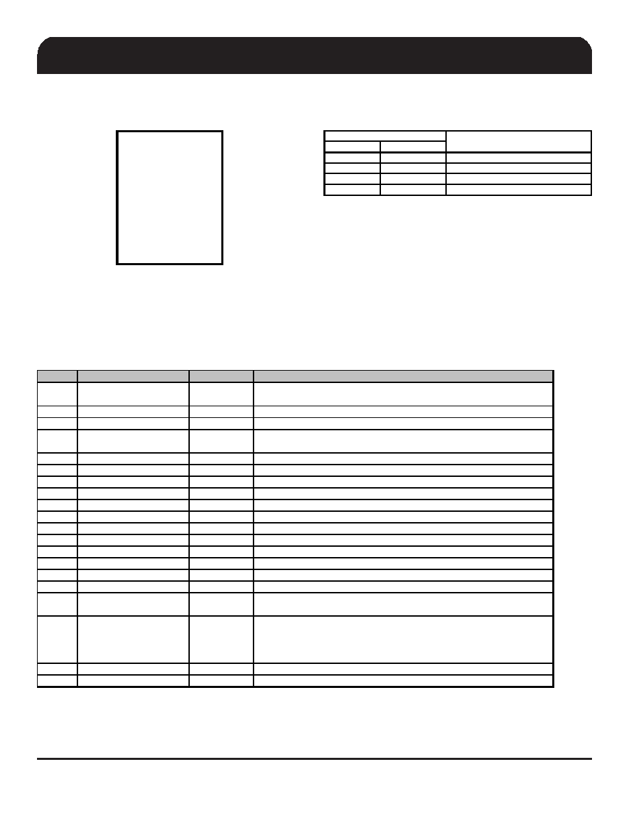
| 型号: | 9DB102AGILF |
| 厂商: | INTEGRATED DEVICE TECHNOLOGY INC |
| 元件分类: | 时钟及定时 |
| 英文描述: | PLL BASED CLOCK DRIVER, PDSO20 |
| 封装: | 4.40 MM, 0.65 MM PITCH, ROHS COMPLIANT, MO-153, TSSOP-20 |
| 文件页数: | 6/13页 |
| 文件大小: | 223K |
| 代理商: | 9DB102AGILF |
IDTTM
Two Output Differential Buffer for PCIe Gen1 & Gen2
852
REV J 01/15/10
ICS9DB102
Two Output Differential Buffer for PCIe Gen1 & Gen2
2
Pin Configuration
PLL_BW 1
20 VDDA
CLK_INT 2
19 GNDA
CLK_INC 3
18 IREF
**CLKREQ0# 417 **CLKREQ1#
VDD 516 VDD
GND 6
15 GND
PCIEXT0 714 PCIEXT1
PCIEXC0 813 PCIEXC1
VDD 912 VDD
SMBDAT 10
11 SMBCLK
IC
S9D
B
102
Note: Pins preceeded by '**' have internal
120K ohm pull down resistors
20-pin SSOP & TSSOP
VDD
GND
5,9,12,16
6,15
PCI Express Outputs
96
SMBUS
20
19
IREF
20
19
Analog VDD & GND for PLL core
Description
Pin Number
Power Groups
Pin Description
PIN #
PIN NAME
PIN TYPE
DESCRIPTION
1
PLL_BW
INPUT
3.3V input for selecting PLL Band Width
0 = low, 1= high
2
CLK_INT
INPUT
"True" reference clock input.
3
CLK_INC
INPUT
"Complementary" reference clock input.
4
**CLKREQ0#
INPUT
Output enable for SRC/PCI Express output pair '0'
0 = enabled, 1 = tri-stated
5
VDD
POWER
Power supply, nominal 3.3V
6
GND
POWER
Ground pin.
7
PCIEXT0
OUTPUT
True clock of differential PCI_Express pair.
8
PCIEXC0
OUTPUT
Complement clock of differential PCI_Express pair.
9
VDD
POWER
Power supply, nominal 3.3V
10
SMBDAT
I/O
Data pin of SMBUS circuitry, 5V tolerant
11
SMBCLK
INPUT
Clock pin of SMBUS circuitry, 5V tolerant
12
VDD
POWER
Power supply, nominal 3.3V
13
PCIEXC1
OUTPUT
Complement clock of differential PCI_Express pair.
14
PCIEXT1
OUTPUT
True clock of differential PCI_Express pair.
15
GND
POWER
Ground pin.
16
VDD
POWER
Power supply, nominal 3.3V
17
**CLKREQ1#
INPUT
Output enable for SRC/PCI Express output pair '1'
0 = enabled, 1 = tri-stated
18
IREF
OUTPUT
This pin establishes the reference current for the differential current-
mode output pairs. This pin requires a fixed precision resistor tied to
ground in order to establish the appropriate current. 475 ohms is the
standard value.
19
GNDA
POWER
Ground pin for the PLL core.
20
VDDA
POWER
3.3V power for the PLL core.
Pins preceeded by '**' have internal 120K ohm pull down resistors
Note:
相关PDF资料 |
PDF描述 |
|---|---|
| 9DB102AGLF | PLL BASED CLOCK DRIVER, PDSO20 |
| 9DB102AFLFT | PLL BASED CLOCK DRIVER, PDSO20 |
| 9DB102AFLF | PLL BASED CLOCK DRIVER, PDSO20 |
| 9DB102AGLFT | PLL BASED CLOCK DRIVER, PDSO20 |
| 9DB102BFILF | 9DB SERIES, PLL BASED CLOCK DRIVER, 2 TRUE OUTPUT(S), 0 INVERTED OUTPUT(S), PDSO20 |
相关代理商/技术参数 |
参数描述 |
|---|---|
| 9DB102BFILF | 制造商:IDT 制造商全称:Integrated Device Technology 功能描述:Two Output Differential Buffer for PCIe Gen1 & Gen2 |
| 9DB102BFILFT | 制造商:IDT 制造商全称:Integrated Device Technology 功能描述:Two Output Differential Buffer for PCIe Gen1 & Gen2 |
| 9DB102BFLF | 功能描述:时钟缓冲器 2 OUTPUT PCIE GEN2 BUFFER RoHS:否 制造商:Texas Instruments 输出端数量:5 最大输入频率:40 MHz 传播延迟(最大值): 电源电压-最大:3.45 V 电源电压-最小:2.375 V 最大功率耗散: 最大工作温度:+ 85 C 最小工作温度:- 40 C 封装 / 箱体:LLP-24 封装:Reel |
| 9DB102BFLFT | 功能描述:时钟缓冲器 2 OUTPUT PCIE GEN2 BUFFER RoHS:否 制造商:Texas Instruments 输出端数量:5 最大输入频率:40 MHz 传播延迟(最大值): 电源电压-最大:3.45 V 电源电压-最小:2.375 V 最大功率耗散: 最大工作温度:+ 85 C 最小工作温度:- 40 C 封装 / 箱体:LLP-24 封装:Reel |
| 9DB102BGILF | 功能描述:时钟缓冲器 2 OUTPUT PCIE GEN2 BUFFER RoHS:否 制造商:Texas Instruments 输出端数量:5 最大输入频率:40 MHz 传播延迟(最大值): 电源电压-最大:3.45 V 电源电压-最小:2.375 V 最大功率耗散: 最大工作温度:+ 85 C 最小工作温度:- 40 C 封装 / 箱体:LLP-24 封装:Reel |
发布紧急采购,3分钟左右您将得到回复。