- 您现在的位置:买卖IC网 > PDF目录25565 > 9DB803DGILFT (INTEGRATED DEVICE TECHNOLOGY INC) 9DB SERIES, PLL BASED CLOCK DRIVER, 8 TRUE OUTPUT(S), 0 INVERTED OUTPUT(S), PDSO48 PDF资料下载
参数资料
| 型号: | 9DB803DGILFT |
| 厂商: | INTEGRATED DEVICE TECHNOLOGY INC |
| 元件分类: | 时钟及定时 |
| 英文描述: | 9DB SERIES, PLL BASED CLOCK DRIVER, 8 TRUE OUTPUT(S), 0 INVERTED OUTPUT(S), PDSO48 |
| 封装: | 6.10 MM, 0.50 MM PITCH, ROHS COMPLIANT, MO-153, TSSOP-48 |
| 文件页数: | 14/21页 |
| 文件大小: | 174K |
| 代理商: | 9DB803DGILFT |
ICS9DB803D
Eight Output Differential Buffer for PCIe Gen 2
21
Innovate with IDT and accelerate your future networks. Contact:
www.IDT.com
For Sales
800-345-7015
408-284-8200
Fax: 408-284-2775
For Tech Support
408-284-6578
pcclockhelp@idt.com
Corporate Headquarters
Integrated Device Technology, Inc.
6024 Silver Creek Valley Road
San Jose, CA 95138
United States
800 345 7015
+408 284 8200 (outside U.S.)
Asia Pacific and Japan
Integrated Device Technology
Singapore (1997) Pte. Ltd.
Reg. No. 199707558G
435 Orchard Road
#20-03 Wisma Atria
Singapore 238877
+65 6 887 5505
Europe
IDT Europe, Limited
Prime House
Barnett Wood Lane
Leatherhead, Surrey
United Kingdom KT22 7DE
+44 1372 363 339
2006 Integrated Device Technology, Inc. All rights reserved. Product specifications subject to change without notice. IDT and the IDT logo are trademarks of Integrated
Device Technology, Inc. Accelerated Thinking is a service mark of Integrated Device Technology, Inc. All other brands, product names and marks are or may be trademarks
or registered trademarks used to identify products or services of their respective owners.
Printed in USA
TM
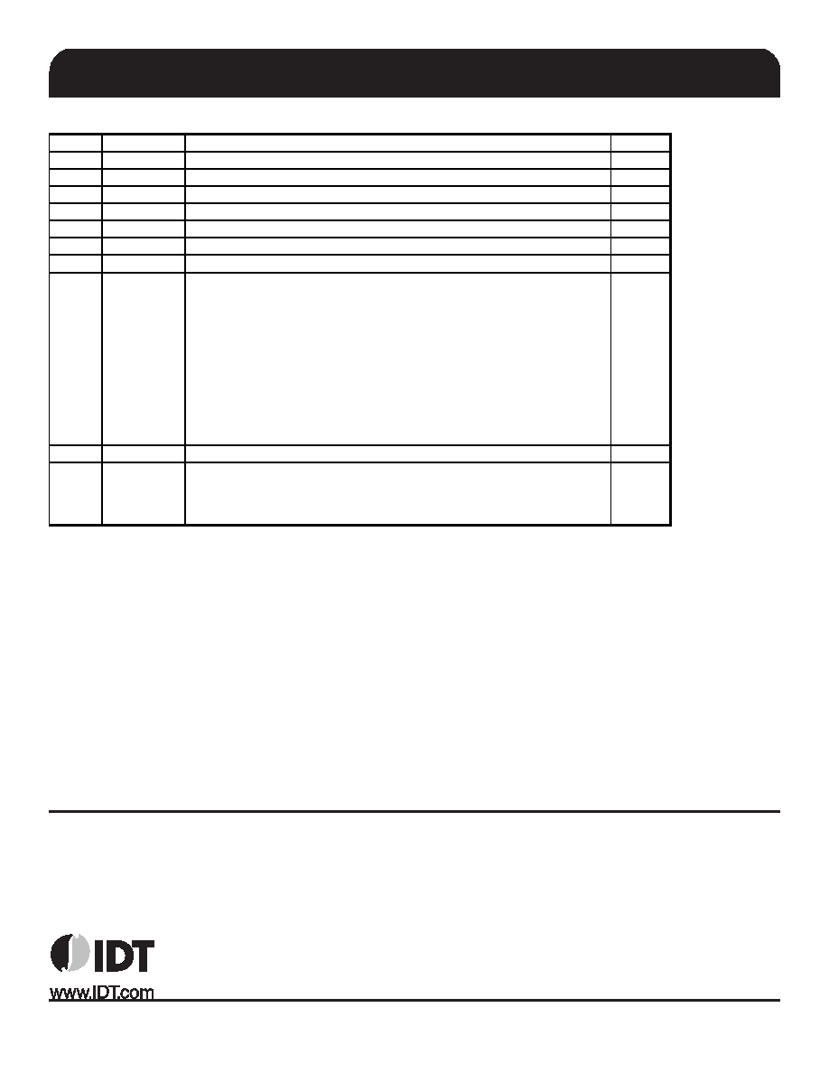
Revision History
Rev.
Issue Date Description
Page #
A
8/15/2006
Updated electrical characteristics for final data sheet
-
B
Added Input Clock Specs
C
2/29/2008
Updated Input Clock Specs
D
3/18/2008
Fixed typo in Input Clock Parameters
E
3/28/2008
Updated Electrical Char tables
F
4/10/2008
Updated Input Clock Specs
G
1/13/2009
Corrected part ordering information
H
10/7/2009
1. Clarified that Vih and Vil values were for Single ended inputs
2. Added Differential Clock input parameters.
3. Updated Electrical Characteristics to add propagation delay and
phase noise information.
4. Added SMBus electrical characteristics
5. Added foot note about DIF input running in order for the SMBus
interface to work
6. Added foot note to Byte 1 about functionality of OE bits and OE
pins.
7. Updated/Reformatted General Description
Various
J
1/27/2011
Updated Termination Figure 4
12
K
5/9/2011
1. Update pin 2 pin-name and pin description from VDD to VDDR. This
highlights that optimal peformance is obtained by treating VDDR as in
analog pin. This is a document update only, there is no silicon change.
Various
相关PDF资料 |
PDF描述 |
|---|---|
| 9DB803DFLF | 9DB SERIES, PLL BASED CLOCK DRIVER, 8 TRUE OUTPUT(S), 0 INVERTED OUTPUT(S), PDSO48 |
| 9DB803DFILF | 9DB SERIES, PLL BASED CLOCK DRIVER, 8 TRUE OUTPUT(S), 0 INVERTED OUTPUT(S), PDSO48 |
| 9DB803DGLF | 9DB SERIES, PLL BASED CLOCK DRIVER, 8 TRUE OUTPUT(S), 0 INVERTED OUTPUT(S), PDSO48 |
| 9DB803DFT | 9DB SERIES, PLL BASED CLOCK DRIVER, 8 TRUE OUTPUT(S), 0 INVERTED OUTPUT(S), PDSO48 |
| 9DB803DGT | 9DB SERIES, PLL BASED CLOCK DRIVER, 8 TRUE OUTPUT(S), 0 INVERTED OUTPUT(S), PDSO48 |
相关代理商/技术参数 |
参数描述 |
|---|---|
| 9DB803DGLF | 功能描述:时钟缓冲器 8 OUTPUT PCIE GEN2 BUFFER RoHS:否 制造商:Texas Instruments 输出端数量:5 最大输入频率:40 MHz 传播延迟(最大值): 电源电压-最大:3.45 V 电源电压-最小:2.375 V 最大功率耗散: 最大工作温度:+ 85 C 最小工作温度:- 40 C 封装 / 箱体:LLP-24 封装:Reel |
| 9DB803DGLFT | 功能描述:时钟缓冲器 8 OUTPUT PCIE GEN2 BUFFER RoHS:否 制造商:Texas Instruments 输出端数量:5 最大输入频率:40 MHz 传播延迟(最大值): 电源电压-最大:3.45 V 电源电压-最小:2.375 V 最大功率耗散: 最大工作温度:+ 85 C 最小工作温度:- 40 C 封装 / 箱体:LLP-24 封装:Reel |
| 9DB823BFLF | 功能描述:时钟缓冲器 8 OUTPUT PCIE GEN2 BUFFER w/QPI RoHS:否 制造商:Texas Instruments 输出端数量:5 最大输入频率:40 MHz 传播延迟(最大值): 电源电压-最大:3.45 V 电源电压-最小:2.375 V 最大功率耗散: 最大工作温度:+ 85 C 最小工作温度:- 40 C 封装 / 箱体:LLP-24 封装:Reel |
| 9DB823BFLFT | 功能描述:时钟缓冲器 8 OUTPUT PCIE GEN2 BUFFER w/QPI RoHS:否 制造商:Texas Instruments 输出端数量:5 最大输入频率:40 MHz 传播延迟(最大值): 电源电压-最大:3.45 V 电源电压-最小:2.375 V 最大功率耗散: 最大工作温度:+ 85 C 最小工作温度:- 40 C 封装 / 箱体:LLP-24 封装:Reel |
| 9DB823BGLF | 功能描述:时钟缓冲器 8 OUTPUT PCIE GEN2 BUFFER w/QPI RoHS:否 制造商:Texas Instruments 输出端数量:5 最大输入频率:40 MHz 传播延迟(最大值): 电源电压-最大:3.45 V 电源电压-最小:2.375 V 最大功率耗散: 最大工作温度:+ 85 C 最小工作温度:- 40 C 封装 / 箱体:LLP-24 封装:Reel |
发布紧急采购,3分钟左右您将得到回复。