- 您现在的位置:买卖IC网 > PDF目录25565 > 9DB803DGILFT (INTEGRATED DEVICE TECHNOLOGY INC) 9DB SERIES, PLL BASED CLOCK DRIVER, 8 TRUE OUTPUT(S), 0 INVERTED OUTPUT(S), PDSO48 PDF资料下载
参数资料
| 型号: | 9DB803DGILFT |
| 厂商: | INTEGRATED DEVICE TECHNOLOGY INC |
| 元件分类: | 时钟及定时 |
| 英文描述: | 9DB SERIES, PLL BASED CLOCK DRIVER, 8 TRUE OUTPUT(S), 0 INVERTED OUTPUT(S), PDSO48 |
| 封装: | 6.10 MM, 0.50 MM PITCH, ROHS COMPLIANT, MO-153, TSSOP-48 |
| 文件页数: | 18/21页 |
| 文件大小: | 174K |
| 代理商: | 9DB803DGILFT |
IDTTM/ICSTM
Eight Output Differential Buffer for PCIe Gen 2
ICS9DB803D
REV K 05/09/11
ICS9DB803D
Eight Output Differential Buffer for PCIe for Gen 2
6
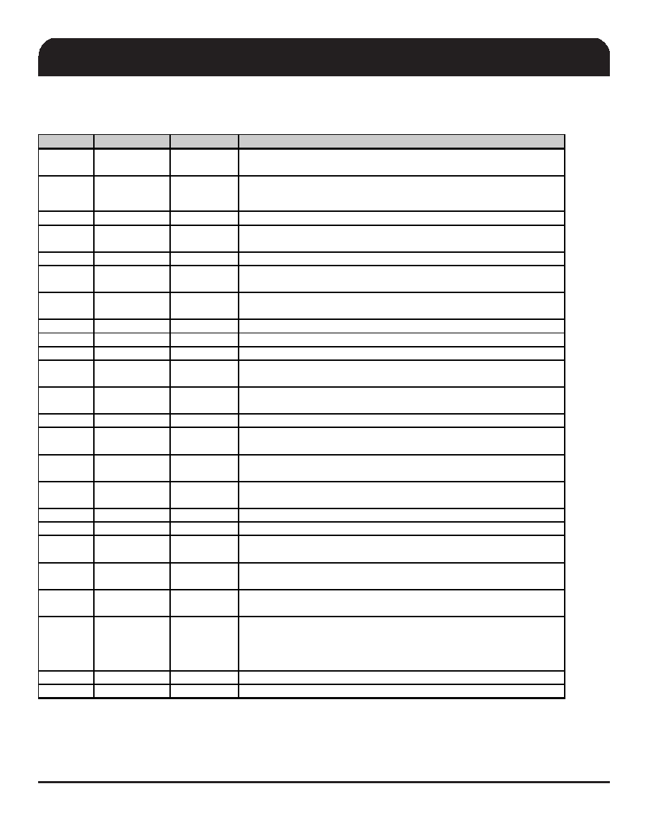
Pin Description for OE_INV = 1
PIN #
PIN NAME
PIN TYPE
DESCRIPTION
25
GND
PWR
Ground pin.
26
PD
IN
Asynchronous active high input pin used to power down the device.
The internal clocks are disabled and the VCO is stopped.
27
DIF_STOP
IN
Active High input to stop differential output clocks.
28
HIGH_BW#
PWR
3.3V input for selecting PLL Band Width
0 = High, 1= Low
29
DIF_4#
OUT
0.7V differential Complementary clock output
30
DIF_4
OUT
0.7V differential true clock output
31
VDD
PWR
Power supply, nominal 3.3V
32
GND
PWR
Ground pin.
33
DIF_5#
OUT
0.7V differential Complementary clock output
34
DIF_5
OUT
0.7V differential true clock output
35
OE5#
IN
Active low input for enabling DIF pair 5.
1 =disable outputs, 0 = enable outputs
36
OE6#
IN
Active low input for enabling DIF pair 6.
1 =disable outputs, 0 = enable outputs
37
DIF_6#
OUT
0.7V differential Complementary clock output
38
DIF_6
OUT
0.7V differential true clock output
39
VDD
PWR
Power supply, nominal 3.3V
40
OE_INV
IN
This latched input selects the polarity of the OE pins.
0 = OE pins active high, 1 = OE pins active low (OE#)
41
DIF_7#
OUT
0.7V differential Complementary clock output
42
DIF_7
OUT
0.7V differential true clock output
43
OE4#
IN
Active low input for enabling DIF pair 4
1 =disable outputs, 0 = enable outputs
44
OE7#
IN
Active low input for enabling DIF pair 7.
1 =disable outputs, 0 = enable outputs
45
LOCK
OUT
3.3V output indicating PLL Lock Status. This pin goes high when lock
is achieved.
46
IREF
IN
This pin establishes the reference for the differential current-mode
output pairs. It requires a fixed precision resistor to ground. 475ohm is
the standard value for 100ohm differential impedance. Other
impedances require different values. See data sheet.
47
GNDA
PWR
Ground pin for the PLL core.
48
VDDA
PWR
3.3V power for the PLL core.
相关PDF资料 |
PDF描述 |
|---|---|
| 9DB803DFLF | 9DB SERIES, PLL BASED CLOCK DRIVER, 8 TRUE OUTPUT(S), 0 INVERTED OUTPUT(S), PDSO48 |
| 9DB803DFILF | 9DB SERIES, PLL BASED CLOCK DRIVER, 8 TRUE OUTPUT(S), 0 INVERTED OUTPUT(S), PDSO48 |
| 9DB803DGLF | 9DB SERIES, PLL BASED CLOCK DRIVER, 8 TRUE OUTPUT(S), 0 INVERTED OUTPUT(S), PDSO48 |
| 9DB803DFT | 9DB SERIES, PLL BASED CLOCK DRIVER, 8 TRUE OUTPUT(S), 0 INVERTED OUTPUT(S), PDSO48 |
| 9DB803DGT | 9DB SERIES, PLL BASED CLOCK DRIVER, 8 TRUE OUTPUT(S), 0 INVERTED OUTPUT(S), PDSO48 |
相关代理商/技术参数 |
参数描述 |
|---|---|
| 9DB803DGLF | 功能描述:时钟缓冲器 8 OUTPUT PCIE GEN2 BUFFER RoHS:否 制造商:Texas Instruments 输出端数量:5 最大输入频率:40 MHz 传播延迟(最大值): 电源电压-最大:3.45 V 电源电压-最小:2.375 V 最大功率耗散: 最大工作温度:+ 85 C 最小工作温度:- 40 C 封装 / 箱体:LLP-24 封装:Reel |
| 9DB803DGLFT | 功能描述:时钟缓冲器 8 OUTPUT PCIE GEN2 BUFFER RoHS:否 制造商:Texas Instruments 输出端数量:5 最大输入频率:40 MHz 传播延迟(最大值): 电源电压-最大:3.45 V 电源电压-最小:2.375 V 最大功率耗散: 最大工作温度:+ 85 C 最小工作温度:- 40 C 封装 / 箱体:LLP-24 封装:Reel |
| 9DB823BFLF | 功能描述:时钟缓冲器 8 OUTPUT PCIE GEN2 BUFFER w/QPI RoHS:否 制造商:Texas Instruments 输出端数量:5 最大输入频率:40 MHz 传播延迟(最大值): 电源电压-最大:3.45 V 电源电压-最小:2.375 V 最大功率耗散: 最大工作温度:+ 85 C 最小工作温度:- 40 C 封装 / 箱体:LLP-24 封装:Reel |
| 9DB823BFLFT | 功能描述:时钟缓冲器 8 OUTPUT PCIE GEN2 BUFFER w/QPI RoHS:否 制造商:Texas Instruments 输出端数量:5 最大输入频率:40 MHz 传播延迟(最大值): 电源电压-最大:3.45 V 电源电压-最小:2.375 V 最大功率耗散: 最大工作温度:+ 85 C 最小工作温度:- 40 C 封装 / 箱体:LLP-24 封装:Reel |
| 9DB823BGLF | 功能描述:时钟缓冲器 8 OUTPUT PCIE GEN2 BUFFER w/QPI RoHS:否 制造商:Texas Instruments 输出端数量:5 最大输入频率:40 MHz 传播延迟(最大值): 电源电压-最大:3.45 V 电源电压-最小:2.375 V 最大功率耗散: 最大工作温度:+ 85 C 最小工作温度:- 40 C 封装 / 箱体:LLP-24 封装:Reel |
发布紧急采购,3分钟左右您将得到回复。