- 您现在的位置:买卖IC网 > PDF目录25565 > 9DB833AGLFT (INTEGRATED DEVICE TECHNOLOGY INC) 9DB SERIES, PLL BASED CLOCK DRIVER, 8 TRUE OUTPUT(S), 0 INVERTED OUTPUT(S), PDSO48 PDF资料下载
参数资料
| 型号: | 9DB833AGLFT |
| 厂商: | INTEGRATED DEVICE TECHNOLOGY INC |
| 元件分类: | 时钟及定时 |
| 英文描述: | 9DB SERIES, PLL BASED CLOCK DRIVER, 8 TRUE OUTPUT(S), 0 INVERTED OUTPUT(S), PDSO48 |
| 封装: | ROHS COMPLIANT, TSSOP-48 |
| 文件页数: | 6/18页 |
| 文件大小: | 226K |
| 代理商: | 9DB833AGLFT |
9DB833
EIGHT OUTPUT DIFFERENTIAL BUFFER FOR PCIE GEN3
IDT
EIGHT OUTPUT DIFFERENTIAL BUFFER FOR PCIE GEN3
14
9DB833
REV C 052411
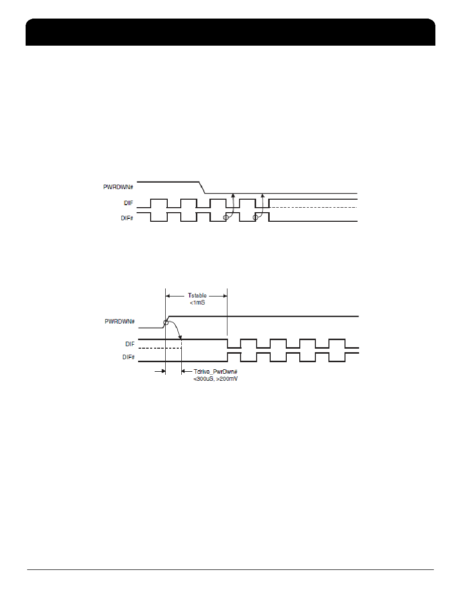
PD#, Power Down
The PD# pin cleanly shuts off all clocks and places the device into a power saving mode. PD# must be asserted before
shutting off the input clock or power to insure an orderly shutdown. PD is asynchronous active-low input for both powering
down the device and powering up the device. When PD# is asserted, all clocks will be driven high, or tri-stated (depending
on the PD# drive mode and Output control bits) before the PLL is shut down.
PD# Assertion
When PD# is sampled low by two consecutive rising edges of DIF#, all DIF outputs must be held High, or tri-stated
(depending on the PD# drive mode and Output control bits) on the next High-Low transition of the DIF# outputs. When the
PD# drive mode bit is set to ‘0’, all clock outputs will be held with DIF driven High with 2 x IREF and DIF# tri-stated. If the PD#
drive mode bit is set to ‘1’, both DIF and DIF# are tri-stated.
PD# De-assertion
Power-up latency is less than 1 ms. This is the time from de-assertion of the PD# pin, or VDD reaching 3.3V, or the time from
valid SRC_IN clocks until the time that stable clocks are output from the device (PLL Locked). If the PD# drive mode bit is
set to ‘1’, all the DIF outputs must driven to a voltage of >200 mV within 300 s of PD# de-assertion.
相关PDF资料 |
PDF描述 |
|---|---|
| 9DB833AGILFT | 9DB SERIES, PLL BASED CLOCK DRIVER, 8 TRUE OUTPUT(S), 0 INVERTED OUTPUT(S), PDSO48 |
| 9DB833AFILFT | 9DB SERIES, PLL BASED CLOCK DRIVER, 8 TRUE OUTPUT(S), 0 INVERTED OUTPUT(S), PDSO48 |
| 9DB833AFLF | 9DB SERIES, PLL BASED CLOCK DRIVER, 8 TRUE OUTPUT(S), 0 INVERTED OUTPUT(S), PDSO48 |
| 9DB833AFLFT | 9DB SERIES, PLL BASED CLOCK DRIVER, 8 TRUE OUTPUT(S), 0 INVERTED OUTPUT(S), PDSO48 |
| 9DBL411AGLFT | LOW SKEW CLOCK DRIVER, PDSO20 |
相关代理商/技术参数 |
参数描述 |
|---|---|
| 9DBL0242BKILF | 功能描述:IC CLK FANOUT/BUFF ZD 24VFQFPN 制造商:idt, integrated device technology inc 系列:- 包装:托盘 零件状态:在售 PLL:是 主要用途:PCI Express(PCIe) 输入:HCSL 输出:HCSL 电路数:1 比率 - 输入:输出:1:2 差分 - 输入:输出:是/是 频率 - 最大值:200MHz 电压 - 电源:3.135 V ~ 3.465 V 工作温度:-40°C ~ 85°C 安装类型:表面贴装 封装/外壳:24-VFQFN 裸露焊盘 供应商器件封装:24-VFQFPN(4x4) 标准包装:490 |
| 9DBL0252BKILF | 功能描述:CLOCK BUFFER 3.3V LP-HCSL PCIE 制造商:idt, integrated device technology inc 系列:* 包装:托盘 零件状态:在售 PLL:是 主要用途:PCI Express(PCIe) 输入:HCSL 输出:HCSL 电路数:1 比率 - 输入:输出:1:2 差分 - 输入:输出:是/是 频率 - 最大值:200MHz 电压 - 电源:3.135 V ~ 3.465 V 工作温度:-40°C ~ 85°C 安装类型:表面贴装 封装/外壳:24-VFQFN 裸露焊盘 供应商器件封装:24-VFQFPN(4x4) 标准包装:490 |
| 9DBL0442BKILF | 功能描述:IC CLK FANOUT/BUFF ZD 32VFQFPN 制造商:idt, integrated device technology inc 系列:- 包装:托盘 零件状态:在售 PLL:是 主要用途:PCI Express(PCIe) 输入:HCSL 输出:HCSL 电路数:1 比率 - 输入:输出:1:4 差分 - 输入:输出:是/是 频率 - 最大值:200MHz 电压 - 电源:3.135 V ~ 3.465 V 工作温度:-40°C ~ 85°C 安装类型:表面贴装 封装/外壳:32-VFQFN 裸露焊盘 供应商器件封装:32-VFQFPN(5x5) 标准包装:490 |
| 9DBL0452BKILF | 功能描述:IC CLK BUFFER ZD 32-VFQFPN 制造商:idt, integrated device technology inc 系列:* 包装:托盘 零件状态:在售 PLL:是 主要用途:PCI Express(PCIe) 输入:HCSL 输出:HCSL 电路数:1 比率 - 输入:输出:1:4 差分 - 输入:输出:是/是 频率 - 最大值:200MHz 电压 - 电源:3.135 V ~ 3.465 V 工作温度:-40°C ~ 85°C 安装类型:表面贴装 封装/外壳:32-VFQFN 裸露焊盘 供应商器件封装:32-VFQFPN(5x5) 标准包装:490 |
| 9DBL0452BKILFT | 功能描述:IC CLK BUFFER ZD 32-VFQFPN 制造商:idt, integrated device technology inc 系列:- 零件状态:在售 PLL:是 主要用途:PCI Express(PCIe) 输入:HCSL 输出:HCSL 电路数:1 比率 - 输入:输出:1:4 差分 - 输入:输出:是/是 频率 - 最大值:200MHz 电压 - 电源:3.135 V ~ 3.465 V 工作温度:-40°C ~ 85°C 安装类型:表面贴装 封装/外壳:32-VFQFN 裸露焊盘 供应商器件封装:32-VFQFPN(5x5) 标准包装:2,500 |
发布紧急采购,3分钟左右您将得到回复。