- 您现在的位置:买卖IC网 > PDF目录25565 > 9FG104DFLF (INTEGRATED DEVICE TECHNOLOGY INC) 400 MHz, PROC SPECIFIC CLOCK GENERATOR, PDSO28 PDF资料下载
参数资料
| 型号: | 9FG104DFLF |
| 厂商: | INTEGRATED DEVICE TECHNOLOGY INC |
| 元件分类: | 时钟产生/分配 |
| 英文描述: | 400 MHz, PROC SPECIFIC CLOCK GENERATOR, PDSO28 |
| 封装: | 0.209 INCH, ROHS COMPLIANT, MO-150, SSOP-28 |
| 文件页数: | 11/17页 |
| 文件大小: | 161K |
| 代理商: | 9FG104DFLF |
IDT
Frequency Generator for CPU, QPI, FBD, PCIe Gen 2 & SATA
1541C—12/16/10
ICS9FG104D
Frequency Generator for CPU, QPI, FBD, PCIe Gen 2 & SATA
3
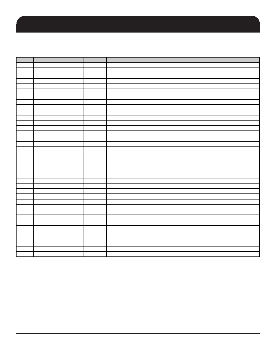
Pin Description
PIN #
PIN NAME
PIN TYPE
DESCRIPTION
1
XIN/CLKIN
IN
Crystal input or Reference Clock input
2
X2
OUT
Crystal output, Nominally 14.318MHz
3
VDD
PWR
Power supply, nominal 3.3V
4
GND
PWR
Ground pin.
5
REFOUT
OUT
Reference Clock output
6
vFS2
IN
3.3V Frequency select latched input pin with internal 120kohm pull down resistor.
7
DIF_3
OUT
0.7V differential true clock output
8
DIF_3#
OUT
0.7V differential Complementary clock output
9
VDD
PWR
Power supply, nominal 3.3V
10
GND
PWR
Ground pin.
11
DIF_2
OUT
0.7V differential true clock output
12
DIF_2#
OUT
0.7V differential Complementary clock output
13
SDATA
I/O
Data pin for SMBus circuitry, 5V tolerant.
14
SCLK
IN
Clock pin of SMBus circuitry, 5V tolerant.
15
DIF_STOP#
IN
Active low input to stop differential output clocks.
16
vSPREAD
IN
Asynchronous, active high input to enable spread spectrum functionality. This pin
has a 120Kohm pull down resistor.
17
^SEL14M_25M#
IN
Select 14.31818 MHz or 25 Mhz input frequency. This pin has an internal 120kohm
pull up resistor.
1 = 14.31818 MHz, 0 = 25 MHz
18
DIF_1#
OUT
0.7V differential Complementary clock output
19
DIF_1
OUT
0.7V differential true clock output
20
GND
PWR
Ground pin.
21
VDD
PWR
Power supply, nominal 3.3V
22
DIF_0#
OUT
0.7V differential Complementary clock output
23
DIF_0
OUT
0.7V differential true clock output
24
vFS1
IN
3.3V Frequency select latched input pin with internal 120kohm pull down resistor.
25
vFS0
IN
3.3V Frequency select latched input pin with internal 120kohm pull down resistor.
26
IREF
OUT
This pin establishes the reference for the differential current-mode output pairs. It
requires a fixed precision resistor to ground. 475ohm is the standard value for
100ohm differential impedance. Other impedances require different values. See
data sheet.
27
GNDA
PWR
Ground pin for the PLL core.
28
VDDA
PWR
3.3V power for the PLL core.
相关PDF资料 |
PDF描述 |
|---|---|
| 9FG104DGILF | 400 MHz, PROC SPECIFIC CLOCK GENERATOR, PDSO28 |
| 9FG104DFILFT | 400 MHz, PROC SPECIFIC CLOCK GENERATOR, PDSO28 |
| 9FG104DGILFT | 400 MHz, PROC SPECIFIC CLOCK GENERATOR, PDSO28 |
| 9FG104DFILF | 400 MHz, PROC SPECIFIC CLOCK GENERATOR, PDSO28 |
| 9FG104DGLF | 400 MHz, PROC SPECIFIC CLOCK GENERATOR, PDSO28 |
相关代理商/技术参数 |
参数描述 |
|---|---|
| 9FG104DFLFT | 功能描述:时钟合成器/抖动清除器 PCIE GEN2 SYNTHESIZER RoHS:否 制造商:Skyworks Solutions, Inc. 输出端数量: 输出电平: 最大输出频率: 输入电平: 最大输入频率:6.1 GHz 电源电压-最大:3.3 V 电源电压-最小:2.7 V 封装 / 箱体:TSSOP-28 封装:Reel |
| 9FG104DGILF | 功能描述:时钟合成器/抖动清除器 PCIE GEN2 SYNTHESIZER RoHS:否 制造商:Skyworks Solutions, Inc. 输出端数量: 输出电平: 最大输出频率: 输入电平: 最大输入频率:6.1 GHz 电源电压-最大:3.3 V 电源电压-最小:2.7 V 封装 / 箱体:TSSOP-28 封装:Reel |
| 9FG104DGILFT | 功能描述:时钟合成器/抖动清除器 PCIE GEN2 SYNTHESIZER RoHS:否 制造商:Skyworks Solutions, Inc. 输出端数量: 输出电平: 最大输出频率: 输入电平: 最大输入频率:6.1 GHz 电源电压-最大:3.3 V 电源电压-最小:2.7 V 封装 / 箱体:TSSOP-28 封装:Reel |
| 9FG104DGLF | 功能描述:时钟合成器/抖动清除器 PCIE GEN2 SYNTHESIZER RoHS:否 制造商:Skyworks Solutions, Inc. 输出端数量: 输出电平: 最大输出频率: 输入电平: 最大输入频率:6.1 GHz 电源电压-最大:3.3 V 电源电压-最小:2.7 V 封装 / 箱体:TSSOP-28 封装:Reel |
| 9FG104DG-LF | 制造商:Integrated Device Technology Inc 功能描述:PROGRAMMABLE PLL FREQ TIMING GENERATOR SGL 28TSSOP - Rail/Tube |
发布紧急采购,3分钟左右您将得到回复。