- 您现在的位置:买卖IC网 > PDF目录25566 > 9FG830AGLF (INTEGRATED DEVICE TECHNOLOGY INC) 400 MHz, PROC SPECIFIC CLOCK GENERATOR, PDSO48 PDF资料下载
参数资料
| 型号: | 9FG830AGLF |
| 厂商: | INTEGRATED DEVICE TECHNOLOGY INC |
| 元件分类: | 时钟产生/分配 |
| 英文描述: | 400 MHz, PROC SPECIFIC CLOCK GENERATOR, PDSO48 |
| 封装: | 6.10 MM, 0.50 MM PITCH, ROHS COMPLIANT, MO-153, TSSOP-48 |
| 文件页数: | 16/19页 |
| 文件大小: | 219K |
| 代理商: | 9FG830AGLF |
IDT Eight Output Differential Frequency Generator for PCIe Gen3 and QPI
1680C—08/26/10
9FG830
Eight Output Differential Frequency Generator for PCIe Gen3 and QPI
6
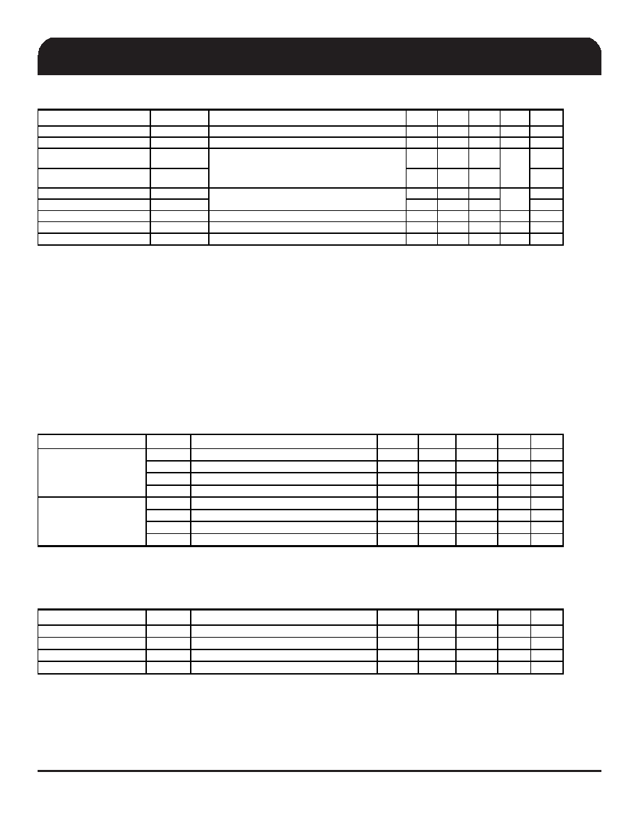
Electrical Characteristics - DIF 0.7V Current Mode Differential Outputs
TA = TCOM or TIND; Supply Voltage VDD = 3.3 V +/-5%, See Test Loads for loading conditions
PARAMETER
SYMBOL
CONDITIONS
MIN
TYP
MAX UNITS NOTES
Slew rate
Trf
Scope averaging on
1
4
V/ns
1, 2, 3
Slew rate matching
Trf
Slew rate matching, Scope averaging on
20
%
1, 2, 4
Voltage High
VHigh
660
850
1
Voltage Low
VLow
-150
150
1
Max Voltage
Vmax
1150
1
Min Voltage
Vmin
-300
1
Vswing
Scope averaging off
300
mV
1, 2
Crossing Voltage (abs)
Vcross_abs
Scope averaging off
250
550
mV
1, 5
Crossing Voltage (var)
-Vcross
Scope averaging off
140
mV
1, 6
2 Measured from differential waveform
6 The total variation of all Vcross measurements in a particular system. This is a subset of V_cross_min/max (V_cross absolute)
allowed. The intent is to limit Vcross induced modulation by setting V_cross_delta to be smaller than V_cross absolute.
mV
Statistical measurement on single-ended signal
using oscilloscope math function. (Scope
averaging on)
Measurement on single ended signal using
absolute value. (Scope averaging off)
mV
1Guaranteed by design and characterization, not 100% tested in production. IREF = VDD/(3xR
R). For RR = 475
(1%), IREF = 2.32mA.
IOH = 6 x IREF and VOH = 0.7V @ ZO=50 (100 differential impedance).
3 Slew rate is measured through the Vswing voltage range centered around differential 0V. This results in a +/-150mV window around
differential 0V.
4 Matching applies to rising edge rate of Clock / falling edge rate of Clock#. It is measured in a +/-75mV window centered on the
average cross point where Clock rising meets Clock# falling. The median cross point is used to calculate the voltage thresholds the
oscilloscope uses for the edge rate calculations.
5 Vcross is defined as voltage where Clock = Clock# measured on a component test board and only applies to the differential rising
edge (i.e. Clock rising and Clock# falling).
Electrical Characteristics - Current Consumption
TA = TCOM or TIND; Supply Voltage VDD = 3.3 V +/-5%, See Test Loads for loading conditions
PARAMETER
SYMBOL
CONDITIONS
MIN
TYP
MAX
UNITS NOTES
IDD3.3
VDD, All outputs active @100MHz
250
mA
1
IDDA3.3OP
VDDA, All outputs active @100MHz
28
mA
1
IDD3.3
VDD, All outputs active @400MHz
200
mA
1
IDDA3.3OP
VDDA, All outputs active @400MHz
28
mA
1
IDD3.3DS
VDD, All DIF pairs stopped driven
190
mA
1
IDDA3.3DS
VDDA, All DIF pairs stopped driven
28
mA
1
IDD3.3DZ
VDD, All DIF pairs stopped Hi-Z
38
mA
1
IDDA3.3DZ
VDDA, All DIF pairs stopped Hi-Z
28
mA
1
1Guaranteed by design and characterization, not 100% tested in production.
2 I
REF = VDD/(3xRR). For RR = 475
(1%), IREF = 2.32mA. IOH = 6 x IREF and VOH = 0.7V @ ZO=50 .
Operating Supply Current
DIF_STOP# Current
Electrical Characteristics - Output Duty Cycle, Jitter, and Skew Characterisitics
TA = TCOM or TIND; Supply Voltage VDD = 3.3 V +/-5%, See Test Loads for Loading Conditions
PARAMETER
SYMBOL
CONDITIONS
MIN
TYP
MAX
UNITS NOTES
Duty Cycle
tDC
Measured differentially, PLL Mode
45
55
%
1
Skew, Output to Output
tsk3
VT = 50%
50
ps
1
Jitter, Cycle to cycle
tjcyc-cyc
25M input
50
ps
1,3
Jitter, Cycle to cycle
tjcyc-cyc
14.318M input
60
ps
1,3
1Guaranteed by design and characterization, not 100% tested in production.
2 I
REF = VDD/(3xRR). For RR = 475
(1%), IREF = 2.32mA. IOH = 6 x IREF and VOH = 0.7V @ ZO=50 .
3 Measured from differential waveform
相关PDF资料 |
PDF描述 |
|---|---|
| 9FGP202AKLFT | 33.33 MHz, OTHER CLOCK GENERATOR, PQCC40 |
| 9G100 | ACTIVE DELAY LINE, TRUE OUTPUT, CDIP4 |
| 9G125S | ACTIVE DELAY LINE, TRUE OUTPUT, CDIP4 |
| 9G125 | ACTIVE DELAY LINE, TRUE OUTPUT, CDIP4 |
| 9G150 | ACTIVE DELAY LINE, TRUE OUTPUT, CDIP4 |
相关代理商/技术参数 |
参数描述 |
|---|---|
| 9FG830AGLFT | 功能描述:时钟发生器及支持产品 PCIE SYNTHESIZER - GEN3, 8 OUTPUT RoHS:否 制造商:Silicon Labs 类型:Clock Generators 最大输入频率:14.318 MHz 最大输出频率:166 MHz 输出端数量:16 占空比 - 最大:55 % 工作电源电压:3.3 V 工作电源电流:1 mA 最大工作温度:+ 85 C 安装风格:SMD/SMT 封装 / 箱体:QFN-56 |
| 9FG831AFILF | 功能描述:时钟合成器/抖动清除器 PCIE SYNTHESIZER - GEN3, 8 OUTPUT RoHS:否 制造商:Skyworks Solutions, Inc. 输出端数量: 输出电平: 最大输出频率: 输入电平: 最大输入频率:6.1 GHz 电源电压-最大:3.3 V 电源电压-最小:2.7 V 封装 / 箱体:TSSOP-28 封装:Reel |
| 9FG831AFILFT | 功能描述:时钟合成器/抖动清除器 PCIE SYNTHESIZER - GEN3, 8 OUTPUT RoHS:否 制造商:Skyworks Solutions, Inc. 输出端数量: 输出电平: 最大输出频率: 输入电平: 最大输入频率:6.1 GHz 电源电压-最大:3.3 V 电源电压-最小:2.7 V 封装 / 箱体:TSSOP-28 封装:Reel |
| 9FG831AFLF | 功能描述:时钟合成器/抖动清除器 PCIE SYNTHESIZER - GEN3, 8 OUTPUT RoHS:否 制造商:Skyworks Solutions, Inc. 输出端数量: 输出电平: 最大输出频率: 输入电平: 最大输入频率:6.1 GHz 电源电压-最大:3.3 V 电源电压-最小:2.7 V 封装 / 箱体:TSSOP-28 封装:Reel |
| 9FG831AFLFT | 功能描述:时钟合成器/抖动清除器 PCIE SYNTHESIZER - GEN3, 8 OUTPUT RoHS:否 制造商:Skyworks Solutions, Inc. 输出端数量: 输出电平: 最大输出频率: 输入电平: 最大输入频率:6.1 GHz 电源电压-最大:3.3 V 电源电压-最小:2.7 V 封装 / 箱体:TSSOP-28 封装:Reel |
发布紧急采购,3分钟左右您将得到回复。