- 您现在的位置:买卖IC网 > PDF目录67355 > A1351KKTTN-T MAGNETIC FIELD SENSOR-HALL EFFECT, 0.20-4.80V, RECTANGULAR, THROUGH HOLE MOUNT PDF资料下载
参数资料
| 型号: | A1351KKTTN-T |
| 元件分类: | 磁阻传感器 |
| 英文描述: | MAGNETIC FIELD SENSOR-HALL EFFECT, 0.20-4.80V, RECTANGULAR, THROUGH HOLE MOUNT |
| 封装: | LEAD FREE, PLASTIC, SIP-4 |
| 文件页数: | 1/23页 |
| 文件大小: | 654K |
| 代理商: | A1351KKTTN-T |
Description
TheA1351 device is a high precision, programmable linear Hall
effect sensor IC with a pulse width modulated (PWM) output.
The duty cycle, D, of the PWM output signal is proportional
to an applied magnetic field. The A1351 device converts an
analog signal from its internal Hall element to a digitally
encoded PWM output signal. The coupled noise immunity of
the digitally encoded PWM output is far superior to the noise
immunity of an analog output signal. A simple RC network
can be used to convert the digital PWM signal back to analog
signal.
The BiCMOS, monolithic circuit inside of theA1351 integrates
a Hall element, precision temperature-compensating circuitry
to reduce the intrinsic sensitivity and offset drift of the Hall
element, a small-signal high-gain amplifier, proprietary
dynamic offset cancellation circuits, and PWM conversion
circuitry. The dynamic offset cancellation circuits reduce
the residual offset voltage of the Hall element. Hall element
offset is normally caused by device over molding, temperature
dependencies, and thermal stress. The high frequency offset
cancellation (chopping) clock allows for a greater sampling
rate, which increases the accuracy of the output signal and
results in faster signal processing capability.
Features and Benefits
Pulse width modulated (PWM) output provides increased noise
immunity compared to an analog output
1 mm case thickness provides greater coupling for current
sensing applications
Push/pull output
Customer-programmable offset and sensitivity
Factory-programmed 0%/°C Sensitivity Temperature Coefficient
Programmability at end-of-line
Selectable unipolar or bipolar quiescent duty cycles
Selectable sensitivity range between 0.055% and 0.095% D/G
Temperature-stable quiescent duty cycle output and sensitivity
Precise recoverability after temperature cycling
Output duty cycle clamps provide short circuit diagnostic
capabilities
Optional 50% D calibration test mode at device power-up
Wide ambient temperature range: –40°C to 125°C
Resistant to mechanical stress
A1351
A1351-DS, Rev. 4
High Precision Linear Hall Effect Sensor IC
with a Push/Pull, Pulse Width Modulated Output
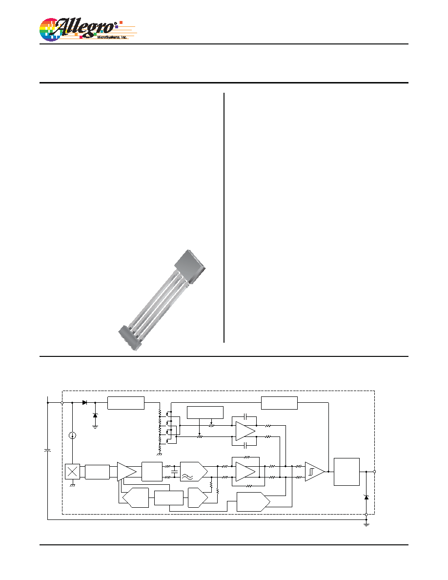
Functional Block Diagram
Continued on the next page…
Package: 4 pin SIP (suffix KT)
Not to scale
VCC
V+
PWMOUT/
Programming
GND
V
REG
C
BYPASS
1
2
1
Temperature
Compensation
Chopper
Switches
PWM
Frequency Trim
Signal
Recovery
PWM Carrier
Generation
PWM
Modulation
Logic with
Push-Pull
Output
Regulator
Signal
Conditioning
% Duty Cycle
Temperature
Coefficient
% Duty
Cycle
Sensitivity
Trim
Amp
1 mm case thickness
相关PDF资料 |
PDF描述 |
|---|---|
| A1354KKTTN-T | MAGNETIC FIELD SENSOR-HALL EFFECT, RECTANGULAR, THROUGH HOLE MOUNT |
| A1382ELHLT-T | MAGNETIC FIELD SENSOR-HALL EFFECT, 4.35-4.65V, RECTANGULAR, SURFACE MOUNT |
| A1381LLHLT-T | MAGNETIC FIELD SENSOR-HALL EFFECT, 4.35-4.65V, RECTANGULAR, SURFACE MOUNT |
| A1384LUA-T | MAGNETIC FIELD SENSOR-HALL EFFECT, 4.35-4.65V, RECTANGULAR, THROUGH HOLE MOUNT |
| A1383EUA-T | MAGNETIC FIELD SENSOR-HALL EFFECT, 4.35-4.65V, RECTANGULAR, THROUGH HOLE MOUNT |
相关代理商/技术参数 |
参数描述 |
|---|---|
| A1351LKTTN-T | 功能描述:IC SENSOR HALL EFFECT 4-SIP RoHS:是 类别:传感器,转换器 >> 磁性 - 霍尔效应,数字式开关,线性,罗盘 (IC) 系列:- 标准包装:1 系列:- 传感范围:20mT ~ 80mT 类型:旋转 电源电压:4.5 V ~ 5.5 V 电流 - 电源:15mA 电流 - 输出(最大):- 输出类型:数字式,PWM,8.5 位串行 特点:可编程 工作温度:-40°C ~ 150°C 封装/外壳:20-SSOP(0.209",5.30mm 宽) 供应商设备封装:20-SSOP 包装:Digi-Reel® 其它名称:AS5132-HSST-500DKR |
| A1352-035 | 制造商:AVX Corporation 功能描述: |
| A1352-037 | 制造商:AVX Corporation 功能描述: |
| A13532-43N | 制造商:Harris Corporation 功能描述: |
| A1354 | 制造商:ALLEGRO 制造商全称:Allegro MicroSystems 功能描述:High Precision 2-Wire Linear Hall Effect Sensor IC with Pulse Width Modulated Output |
发布紧急采购,3分钟左右您将得到回复。