- 您现在的位置:买卖IC网 > PDF目录294784 > A1425A-1PL84C FPGA, 310 CLBS, 2500 GATES, 150 MHz, PQCC84 PDF资料下载
参数资料
| 型号: | A1425A-1PL84C |
| 元件分类: | FPGA |
| 英文描述: | FPGA, 310 CLBS, 2500 GATES, 150 MHz, PQCC84 |
| 封装: | PLASTIC, LCC-84 |
| 文件页数: | 56/68页 |
| 文件大小: | 489K |
| 代理商: | A1425A-1PL84C |
第1页第2页第3页第4页第5页第6页第7页第8页第9页第10页第11页第12页第13页第14页第15页第16页第17页第18页第19页第20页第21页第22页第23页第24页第25页第26页第27页第28页第29页第30页第31页第32页第33页第34页第35页第36页第37页第38页第39页第40页第41页第42页第43页第44页第45页第46页第47页第48页第49页第50页第51页第52页第53页第54页第55页当前第56页第57页第58页第59页第60页第61页第62页第63页第64页第65页第66页第67页第68页
1-180
Hermetic Device Resources
Pin Description
CLKA
Clock A (Input)
Clock input for clock distribution networks. The Clock input
is buffered prior to clocking the logic modules. This pin can
also be used as an I/O.
CLKB
Clock B (Input)
Clock input for clock distribution networks. The Clock input
is buffered prior to clocking the logic modules. This pin can
also be used as an I/O.
GND
Ground
LOW supply voltage.
HCLK
Dedicated (Hard-wired)
Array Clock (Input)
Clock input for sequential modules. This input is directly
wired to each S-Module and offers clock speeds independent
of the number of S-Modules being driven. This pin can also be
used as an I/O.
I/O
Input/Output (Input, Output)
The I/O pin functions as an input, output, three-state, or
bidirectional buffer. Input and output levels are compatible
with standard TTL and CMOS specifications. Unused I/O pins
are tristated by the Designer Series software.
IOCLK
Dedicated (Hard-wired)
I/O Clock (Input)
Clock input for I/O modules. This input is directly wired to
each I/O module and offers clock speeds independent of the
number of I/O modules being driven. This pin can also be
used as an I/O.
IOPCL
Dedicated (Hard-wired)
I/O Preset/Clear (Input)
Input for I/O preset or clear. This global input is directly
wired to the preset and clear inputs of all I/O registers. This
pin functions as an I/O when no I/O preset or clear macros
are used.
MODE
Mode (Input)
The MODE pin controls the use of diagnostic pins (DCLK,
PRA, PRB, SDI). When the MODE pin is HIGH, the special
functions are active. When the MODE pin is LOW, the pins
function as I/Os. To provide Actionprobe capability, the
MODE pin should be terminated to GND through a 10K
resistor so that the MODE pin can be pulled high when
required.
NC
No Connection
This pin is not connected to circuitry within the device.
PRA
Probe A (Output)
The Probe A pin is used to output data from any user-defined
design node within the device. This independent diagnostic
pin can be used in conjunction with the Probe B pin to allow
real-time diagnostic output of any signal path within the
device. The Probe A pin can be used as a user-defined I/O
when debugging has been completed. The pin’s probe
capabilities can be permanently disabled to protect
programmed design confidentiality. PRA is accessible when
the MODE pin is HIGH. This pin functions as an I/O when the
MODE pin is LOW.
PRB
Probe B (Output)
The Probe B pin is used to output data from any user-defined
design node within the device. This independent diagnostic
pin can be used in conjunction with the Probe A pin to allow
real-time diagnostic output of any signal path within the
device. The Probe B pin can be used as a user-defined I/O
when debugging has been completed. The pin’s probe
capabilities can be permanently disabled to protect
programmed design confidentiality. PRB is accessible when
the MODE pin is HIGH. This pin functions as an I/O when the
MODE pin is LOW.
SDI
Serial Data Input (Input)
Serial
data
input
for
diagnostic
probe
and
device
programming. SDI is active when the MODE pin is HIGH. This
pin functions as an I/O when the MODE pin is LOW.
DCLK
Diagnostic Clock (Input)
Clock input for diagnostic probe and device programming.
DCLK is active when the MODE pin is HIGH. This pin
functions as an I/O when the MODE pin is LOW.
VCC
5 V Supply Voltage
HIGH supply voltage.
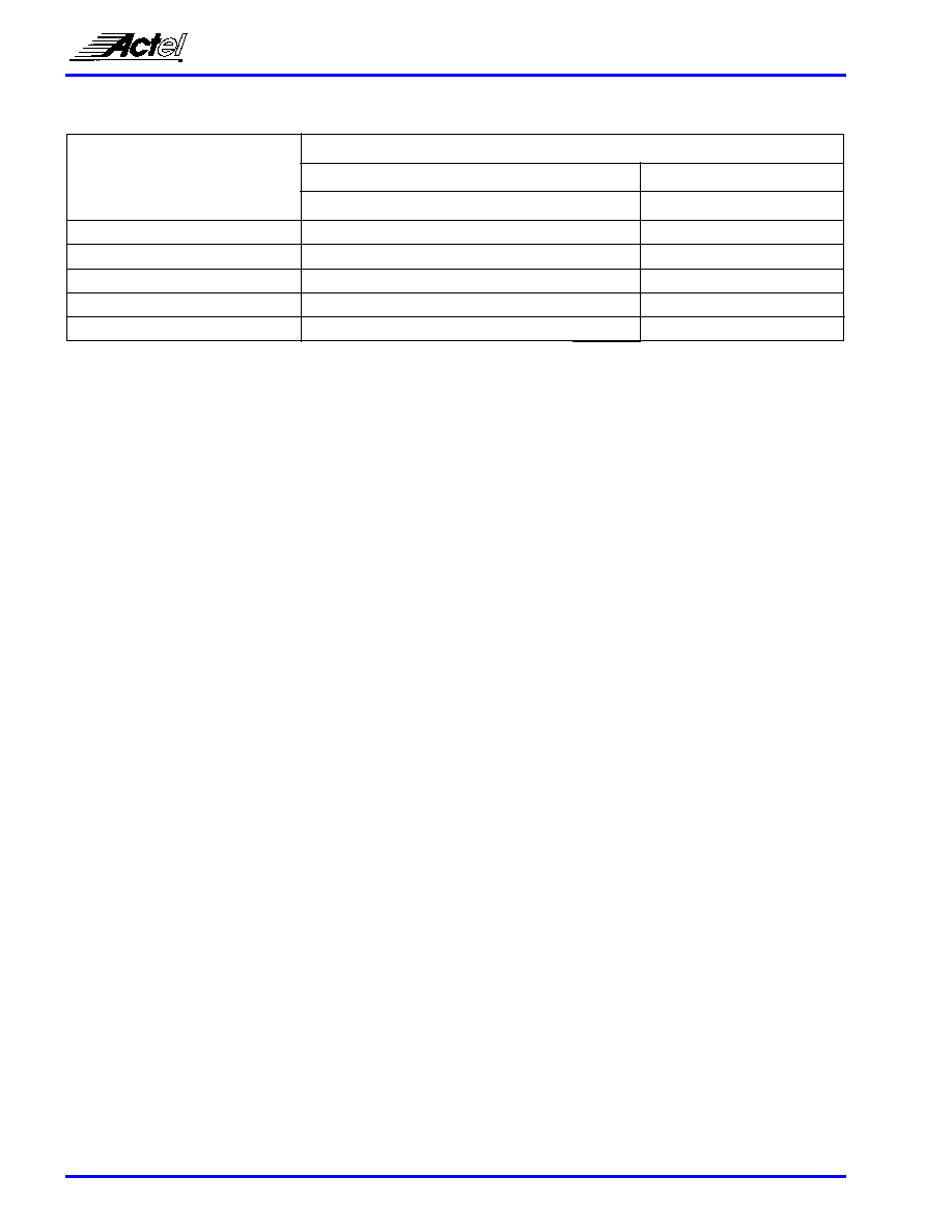
Device
Series
Logic
Modules
User I/Os
CPGA
CQFP
Gates
100-pin
133-pin
175-pin
207-pin
257-pin
132-pin
196-pin
256-pin
A1415
200
1500
80
—
A1425
310
2500
—
100
—
100
—
A1440
564
4000
—
140
—
A1460
848
6000
—
168
—
168
—
A14100
1377
10000
—
228
—
228
相关PDF资料 |
PDF描述 |
|---|---|
| A1425A-1PL84I | FPGA, 310 CLBS, 2500 GATES, PQCC84 |
| A1425A-1PLG84C | FPGA, 310 CLBS, 2500 GATES, 150 MHz, PQCC84 |
| A1425A-1PLG84I | FPGA, 310 CLBS, 2500 GATES, PQCC84 |
| A1425A-1PQ100C | FPGA, 310 CLBS, 2500 GATES, 150 MHz, PQFP100 |
| A1425A-1PQ100I | FPGA, 310 CLBS, 2500 GATES, PQFP100 |
相关代理商/技术参数 |
参数描述 |
|---|---|
| A1425A-1PL84I | 功能描述:IC FPGA 2500 GATES 84-PLCC RoHS:否 类别:集成电路 (IC) >> 嵌入式 - FPGA(现场可编程门阵列) 系列:ACT™ 3 产品变化通告:XC4000(E,L) Discontinuation 01/April/2002 标准包装:24 系列:XC4000E/X LAB/CLB数:100 逻辑元件/单元数:238 RAM 位总计:3200 输入/输出数:80 门数:3000 电源电压:4.5 V ~ 5.5 V 安装类型:表面贴装 工作温度:-40°C ~ 100°C 封装/外壳:120-BCBGA 供应商设备封装:120-CPGA(34.55x34.55) |
| A1425A-1PLG84C | 功能描述:IC FPGA 2500 GATES 84-PLCC RoHS:是 类别:集成电路 (IC) >> 嵌入式 - FPGA(现场可编程门阵列) 系列:ACT™ 3 产品变化通告:XC4000(E,L) Discontinuation 01/April/2002 标准包装:24 系列:XC4000E/X LAB/CLB数:100 逻辑元件/单元数:238 RAM 位总计:3200 输入/输出数:80 门数:3000 电源电压:4.5 V ~ 5.5 V 安装类型:表面贴装 工作温度:-40°C ~ 100°C 封装/外壳:120-BCBGA 供应商设备封装:120-CPGA(34.55x34.55) |
| A1425A-1PLG84I | 功能描述:IC FPGA 2500 GATES 84-PLCC RoHS:是 类别:集成电路 (IC) >> 嵌入式 - FPGA(现场可编程门阵列) 系列:ACT™ 3 产品变化通告:XC4000(E,L) Discontinuation 01/April/2002 标准包装:24 系列:XC4000E/X LAB/CLB数:100 逻辑元件/单元数:238 RAM 位总计:3200 输入/输出数:80 门数:3000 电源电压:4.5 V ~ 5.5 V 安装类型:表面贴装 工作温度:-40°C ~ 100°C 封装/外壳:120-BCBGA 供应商设备封装:120-CPGA(34.55x34.55) |
| A1425A1PQ100C | 制造商:Microsemi SOC Products Group 功能描述:Field-Programmable Gate Array, 310 Cell, 100 Pin, Plastic, QFP |
| A1425A-1PQ100C | 功能描述:IC FPGA 2500 GATES 100-PQFP RoHS:否 类别:集成电路 (IC) >> 嵌入式 - FPGA(现场可编程门阵列) 系列:ACT™ 3 产品变化通告:XC4000(E,L) Discontinuation 01/April/2002 标准包装:24 系列:XC4000E/X LAB/CLB数:100 逻辑元件/单元数:238 RAM 位总计:3200 输入/输出数:80 门数:3000 电源电压:4.5 V ~ 5.5 V 安装类型:表面贴装 工作温度:-40°C ~ 100°C 封装/外壳:120-BCBGA 供应商设备封装:120-CPGA(34.55x34.55) |
发布紧急采购,3分钟左右您将得到回复。