- 您现在的位置:买卖IC网 > PDF目录294784 > A1425A-1PL84C FPGA, 310 CLBS, 2500 GATES, 150 MHz, PQCC84 PDF资料下载
参数资料
| 型号: | A1425A-1PL84C |
| 元件分类: | FPGA |
| 英文描述: | FPGA, 310 CLBS, 2500 GATES, 150 MHz, PQCC84 |
| 封装: | PLASTIC, LCC-84 |
| 文件页数: | 7/68页 |
| 文件大小: | 489K |
| 代理商: | A1425A-1PL84C |
第1页第2页第3页第4页第5页第6页当前第7页第8页第9页第10页第11页第12页第13页第14页第15页第16页第17页第18页第19页第20页第21页第22页第23页第24页第25页第26页第27页第28页第29页第30页第31页第32页第33页第34页第35页第36页第37页第38页第39页第40页第41页第42页第43页第44页第45页第46页第47页第48页第49页第50页第51页第52页第53页第54页第55页第56页第57页第58页第59页第60页第61页第62页第63页第64页第65页第66页第67页第68页
1-189
Accelerator Series FPGAs – ACT 3 Family
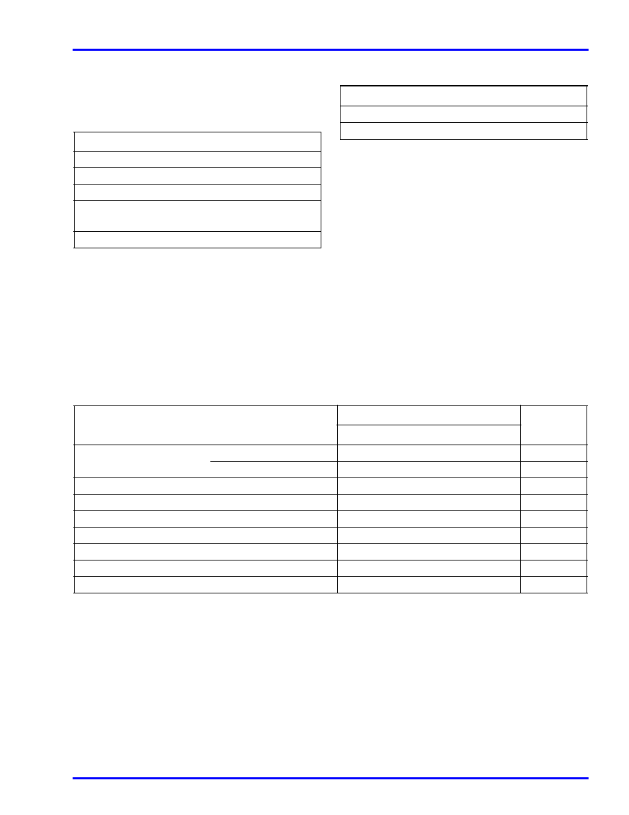
3.3V Operating Conditions
Absolute Maximum Ratings 1
Free air temperature range
Recommended Operating Conditions
Electrical Specifications
Symbol
Parameter
Limits
Units
VCC
DC Supply Voltage
–0.5 to +7.0
V
VI
Input Voltage
–0.5 to VCC +0.5
V
VO
Output Voltage
–0.5 to VCC +0.5
V
IIO
I/O Source Sink
Current2
±20
mA
TSTG
Storage Temperature
–65 to +150
°C
Notes:
1.
Stresses beyond those listed under “Absolute Maximum
Ratings” may cause permanent damage to the device. Exposure
to absolute maximum rated conditions for extended periods
may affect device reliability. Device should not be operated
outside the Recommended Operating Conditions.
2.
Device inputs are normally high impedance and draw
extremely low current. However, when input voltage is greater
than VCC + 0.5 V or less than GND – 0.5 V, the internal
protection diodes will forward bias and can draw excessive
current.
Parameter
Commercial
Units
Temperature Range1
0 to +70
°C
Power Supply Tolerance
3.0 to 3.6
V
Note:
1.
Ambient temperature (TA) is used for commercial.
Parameter
Commercial
Units
Min.
Max.
VOH
1
(IOH = –4 mA)
2.15
V
(IOH = –3.2 mA)
2.4
V
VOL
1
(IOL = 6 mA)
0.4
V
VIL
–0.3
0.8
V
VIH
2.0
VCC + 0.3
V
Input Transition Time tR, tF
2
500
ns
CIO I/O Capacitance
2, 3
10
pF
Standby Current, ICC
4 (typical = 0.3 mA)
0.75
mA
Leakage Current5
–10
10
A
Notes:
1.
Only one output tested at a time. VCC = min.
2.
Not tested, for information only.
3.
Includes worst-case 84-pin PLCC package capacitance. VOUT = 0 V, f = 1 MHz.
4.
Typical standby current = 0.3 mA. All outputs unloaded. All inputs = VCC or GND.
5.
VO, VIN = VCC or GND.
相关PDF资料 |
PDF描述 |
|---|---|
| A1425A-1PL84I | FPGA, 310 CLBS, 2500 GATES, PQCC84 |
| A1425A-1PLG84C | FPGA, 310 CLBS, 2500 GATES, 150 MHz, PQCC84 |
| A1425A-1PLG84I | FPGA, 310 CLBS, 2500 GATES, PQCC84 |
| A1425A-1PQ100C | FPGA, 310 CLBS, 2500 GATES, 150 MHz, PQFP100 |
| A1425A-1PQ100I | FPGA, 310 CLBS, 2500 GATES, PQFP100 |
相关代理商/技术参数 |
参数描述 |
|---|---|
| A1425A-1PL84I | 功能描述:IC FPGA 2500 GATES 84-PLCC RoHS:否 类别:集成电路 (IC) >> 嵌入式 - FPGA(现场可编程门阵列) 系列:ACT™ 3 产品变化通告:XC4000(E,L) Discontinuation 01/April/2002 标准包装:24 系列:XC4000E/X LAB/CLB数:100 逻辑元件/单元数:238 RAM 位总计:3200 输入/输出数:80 门数:3000 电源电压:4.5 V ~ 5.5 V 安装类型:表面贴装 工作温度:-40°C ~ 100°C 封装/外壳:120-BCBGA 供应商设备封装:120-CPGA(34.55x34.55) |
| A1425A-1PLG84C | 功能描述:IC FPGA 2500 GATES 84-PLCC RoHS:是 类别:集成电路 (IC) >> 嵌入式 - FPGA(现场可编程门阵列) 系列:ACT™ 3 产品变化通告:XC4000(E,L) Discontinuation 01/April/2002 标准包装:24 系列:XC4000E/X LAB/CLB数:100 逻辑元件/单元数:238 RAM 位总计:3200 输入/输出数:80 门数:3000 电源电压:4.5 V ~ 5.5 V 安装类型:表面贴装 工作温度:-40°C ~ 100°C 封装/外壳:120-BCBGA 供应商设备封装:120-CPGA(34.55x34.55) |
| A1425A-1PLG84I | 功能描述:IC FPGA 2500 GATES 84-PLCC RoHS:是 类别:集成电路 (IC) >> 嵌入式 - FPGA(现场可编程门阵列) 系列:ACT™ 3 产品变化通告:XC4000(E,L) Discontinuation 01/April/2002 标准包装:24 系列:XC4000E/X LAB/CLB数:100 逻辑元件/单元数:238 RAM 位总计:3200 输入/输出数:80 门数:3000 电源电压:4.5 V ~ 5.5 V 安装类型:表面贴装 工作温度:-40°C ~ 100°C 封装/外壳:120-BCBGA 供应商设备封装:120-CPGA(34.55x34.55) |
| A1425A1PQ100C | 制造商:Microsemi SOC Products Group 功能描述:Field-Programmable Gate Array, 310 Cell, 100 Pin, Plastic, QFP |
| A1425A-1PQ100C | 功能描述:IC FPGA 2500 GATES 100-PQFP RoHS:否 类别:集成电路 (IC) >> 嵌入式 - FPGA(现场可编程门阵列) 系列:ACT™ 3 产品变化通告:XC4000(E,L) Discontinuation 01/April/2002 标准包装:24 系列:XC4000E/X LAB/CLB数:100 逻辑元件/单元数:238 RAM 位总计:3200 输入/输出数:80 门数:3000 电源电压:4.5 V ~ 5.5 V 安装类型:表面贴装 工作温度:-40°C ~ 100°C 封装/外壳:120-BCBGA 供应商设备封装:120-CPGA(34.55x34.55) |
发布紧急采购,3分钟左右您将得到回复。