- 您现在的位置:买卖IC网 > PDF目录17042 > A3PE-STARTER-KIT-2 (Microsemi SoC)KIT EVAL FOR A3PE1500 PROASIC3 PDF资料下载
参数资料
| 型号: | A3PE-STARTER-KIT-2 |
| 厂商: | Microsemi SoC |
| 文件页数: | 110/162页 |
| 文件大小: | 0K |
| 描述: | KIT EVAL FOR A3PE1500 PROASIC3 |
| 产品变化通告: | Kit/Part Number Change 25/Jul/2012 |
| 标准包装: | 1 |
| 系列: | ProASIC3 |
| 类型: | FPGA |
| 适用于相关产品: | A3PE1500 |
| 所含物品: | 板,电源,编程器 |
| 其它名称: | 1100-1144 A3PE-STARTER-KIT |
第1页第2页第3页第4页第5页第6页第7页第8页第9页第10页第11页第12页第13页第14页第15页第16页第17页第18页第19页第20页第21页第22页第23页第24页第25页第26页第27页第28页第29页第30页第31页第32页第33页第34页第35页第36页第37页第38页第39页第40页第41页第42页第43页第44页第45页第46页第47页第48页第49页第50页第51页第52页第53页第54页第55页第56页第57页第58页第59页第60页第61页第62页第63页第64页第65页第66页第67页第68页第69页第70页第71页第72页第73页第74页第75页第76页第77页第78页第79页第80页第81页第82页第83页第84页第85页第86页第87页第88页第89页第90页第91页第92页第93页第94页第95页第96页第97页第98页第99页第100页第101页第102页第103页第104页第105页第106页第107页第108页第109页当前第110页第111页第112页第113页第114页第115页第116页第117页第118页第119页第120页第121页第122页第123页第124页第125页第126页第127页第128页第129页第130页第131页第132页第133页第134页第135页第136页第137页第138页第139页第140页第141页第142页第143页第144页第145页第146页第147页第148页第149页第150页第151页第152页第153页第154页第155页第156页第157页第158页第159页第160页第161页第162页
ProASIC3E Flash Family FPGAs
Revision 13
2-37
3.3 V PCI, 3.3 V PCI-X
Peripheral Component Interface for 3.3 V standard specifies support for 33 MHz and 66 MHz PCI Bus
applications.
AC loadings are defined per the PCI/PCI-X specifications for the datapath; Microsemi loadings for enable
path characterization are described in Figure 2-11.
AC loadings are defined per PCI/PCI-X specifications for the datapath; Microsemi loading for tristate is
described in Table 2-46.
Timing Characteristics
Table 2-45 Minimum and Maximum DC Input and Output Levels
3.3 V PCI/PCI-X
VIL
VIH
VOL
VOH IOL IOH
IOSL
IOSH
IIL1 IIH2
Drive Strength
Min.
V
Max.
V
Min.
V
Max.
V
Max.
V
Min.
VmA mA
Max.
mA3
Max.
mA3
A4 A4
Per PCI specification
Per PCI curves
10 10
Notes:
1. IIL is the input leakage current per I/O pin over recommended operation conditions where –0.3 V< VIN < VIL.
2. IIH is the input leakage current per I/O pin over recommended operating conditions VIH < VIN< VCCI. Input current is
larger when operating outside recommended ranges.
3. Currents are measured at high temperature (100°C junction temperature) and maximum voltage.
4. Currents are measured at 85°C junction temperature.
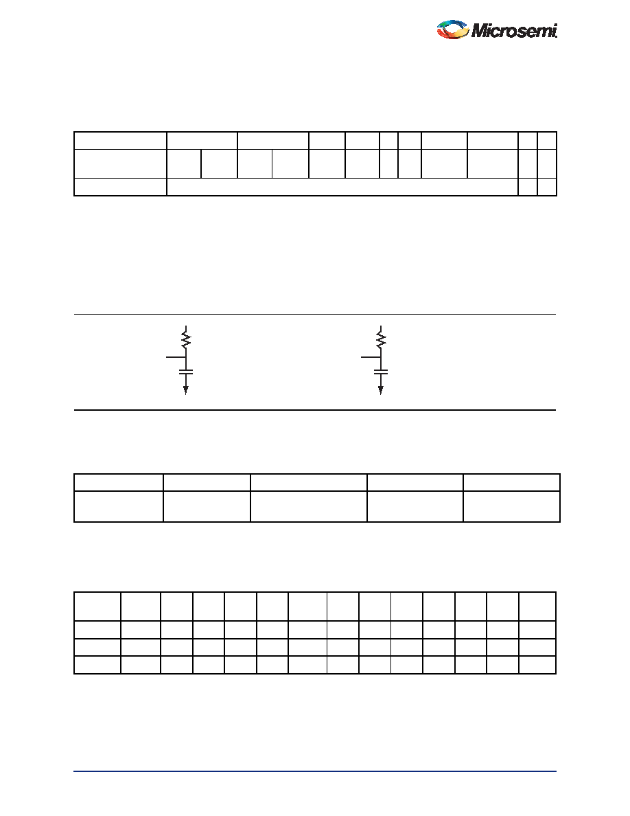
Figure 2-11 AC Loading
Test Point
Enable Path
R to VCCI for tLZ / tZL / tZLS
10 pF for tZH / tZHS / tZL / tZLS
10 pF for tHZ / tLZ
R to GND for tHZ / tZH / tZHS
R = 1 k
Test Point
Datapath
R = 25
R to VCCI for tDP (F)
R to GND for tDP (R)
Table 2-46 AC Waveforms, Measuring Points, and Capacitive Loads
Input Low (V)
Input High (V)
Measuring Point* (V)
VREF (typ.) (V)
CLOAD (pF)
0
3.3
0.285 * VCCI for tDP(R)
0.615 * VCCI for tDP(F)
–10
Note: *Measuring point = Vtrip. See Table 2-15 on page 2-18 for a complete table of trip points.
Table 2-47 3.3 V PCI/PCI-X
Commercial-Case Conditions: TJ = 70°C, Worst-Case VCC = 1.425 V, Worst-Case VCCI = 3.0 V
Speed
Grade
tDOUT
tDP
tDIN
tPY
tPYS
tEOUT
tZL
tZH
tLZ
tHZ
tZLS
tZHS
Units
Std.
0.66
2.81
0.04
1.05
1.67
0.43
2.86
2.00
3.28
3.61
5.09
4.23
ns
–1
0.56
2.39
0.04
0.89
1.42
0.36
2.43
1.70
2.79
3.07
4.33
3.60
ns
–2
0.49
2.09
0.03
0.78
1.25
0.32
2.13
1.49
2.45
2.70
3.80
3.16
ns
Note: For specific junction temperature and voltage supply levels, refer to Table 2-6 on page 2-5 for derating values.
相关PDF资料 |
PDF描述 |
|---|---|
| 0210490279 | CABLE JUMPER 1.25MM .051M 22POS |
| EBM22DCMD-S288 | CONN EDGECARD 44POS .156 EXTEND |
| ECA14DRMI-S288 | CONN EDGECARD 28POS .125 EXTEND |
| 0210490905 | CABLE JUMPER 1.25MM .102M 21POS |
| MPC8377E-RDBA | BOARD REF DES MPC8377 REV 2.1 |
相关代理商/技术参数 |
参数描述 |
|---|---|
| A3PFA1X201J1 | 制造商:APEM 功能描述:Pushbutton,A3,latching,12V,red |
| A3PFA1X201J2 | 制造商:APEM 功能描述:Pushbutton,latching,12V,green |
| A3PFA1X201J3 | 制造商:APEM 功能描述:Pushbutton,latching,12V,amber |
| A3PFA1X201J4 | 制造商:APEM 功能描述:Pushbutton,A3,latching,12V,blue |
| A3PFA1X201K1 | 制造商:APEM 功能描述:Pushbutton,A3,latching 24V,red |
发布紧急采购,3分钟左右您将得到回复。