- 您现在的位置:买卖IC网 > PDF目录164971 > A3PE1500-PQG208 FPGA, 38400 CLBS, 1500000 GATES, PQFP208 PDF资料下载
参数资料
| 型号: | A3PE1500-PQG208 |
| 元件分类: | FPGA |
| 英文描述: | FPGA, 38400 CLBS, 1500000 GATES, PQFP208 |
| 封装: | 28 X 28 MM, 3.40 MM HEIGHT, 0.50 MM PITCH, GREEN, PLASTIC, QFP-208 |
| 文件页数: | 129/152页 |
| 文件大小: | 4932K |
| 代理商: | A3PE1500-PQG208 |
第1页第2页第3页第4页第5页第6页第7页第8页第9页第10页第11页第12页第13页第14页第15页第16页第17页第18页第19页第20页第21页第22页第23页第24页第25页第26页第27页第28页第29页第30页第31页第32页第33页第34页第35页第36页第37页第38页第39页第40页第41页第42页第43页第44页第45页第46页第47页第48页第49页第50页第51页第52页第53页第54页第55页第56页第57页第58页第59页第60页第61页第62页第63页第64页第65页第66页第67页第68页第69页第70页第71页第72页第73页第74页第75页第76页第77页第78页第79页第80页第81页第82页第83页第84页第85页第86页第87页第88页第89页第90页第91页第92页第93页第94页第95页第96页第97页第98页第99页第100页第101页第102页第103页第104页第105页第106页第107页第108页第109页第110页第111页第112页第113页第114页第115页第116页第117页第118页第119页第120页第121页第122页第123页第124页第125页第126页第127页第128页当前第129页第130页第131页第132页第133页第134页第135页第136页第137页第138页第139页第140页第141页第142页第143页第144页第145页第146页第147页第148页第149页第150页第151页第152页
ProASIC3E DC and Switching Characteristics
2- 66
v1.2
Timing Characteristics
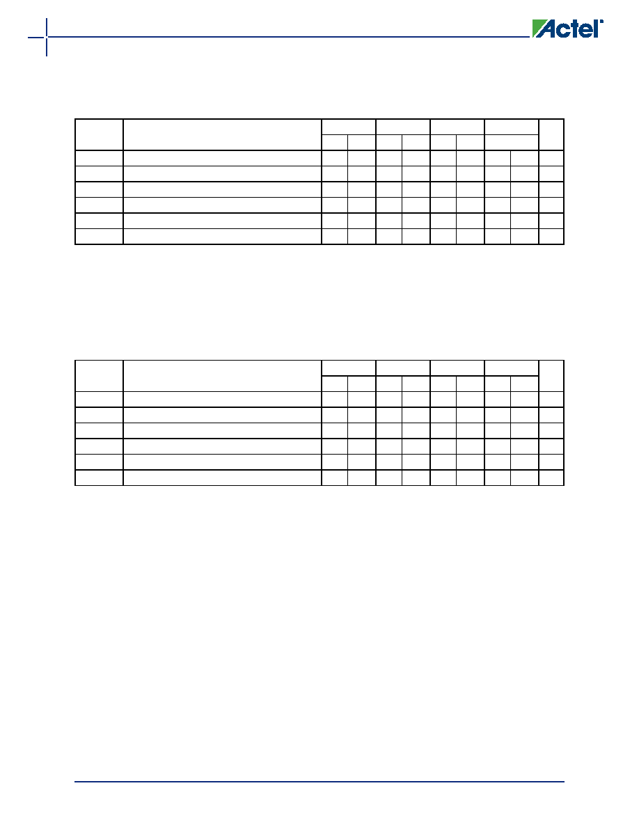
Table 2-91 A3PE600 Global Resource
Commercial-Case Conditions: TJ = 70°C, VCC = 1.425 V
Parameter
Description
–2
–1
Std.
–F
Units
Min.1 Max.2 Min.1 Max.2 Min.1 Max.2 Min.1 Max.2
tRCKL
Input LOW Delay for Global Clock
0.83 1.04 0.94 1.18 1.11 1.39 1.33 1.67
ns
tRCKH
Input HIGH Delay for Global Clock
0.81 1.06 0.93 1.21 1.09 1.42 1.31 1.71
ns
tRCKMPWH Minimum Pulse Width HIGH for Global Clock
ns
tRCKMPWL Minimum Pulse Width LOW for Global Clock
ns
tRCKSW
Maximum Skew for Global Clock
0.25
0.28
0.33
0.40
ns
FRMAX
Maximum Frequency for Global Clock
MHz
Notes:
1. Value reflects minimum load. The delay is measured from the CCC output to the clock pin of a sequential
element, located in a lightly loaded row (single element is connected to the global net).
2. Value reflects maximum load. The delay is measured on the clock pin of the farthest sequential element,
located in a fully loaded row (all available flip-flops are connected to the global net in the row).
3. For specific junction temperature and voltage supply levels, refer to Table 2-6 on page 2-5 for derating values.
Table 2-92 A3PE1500 Global Resource
Commercial-Case Conditions: TJ = 70°C, VCC = 1.425 V
Parameter
Description
–2
–1
Std.
–F
Units
Min.1 Max.2 Min.1 Max.2 Min.1 Max.2 Min.1 Max.2
tRCKL
Input LOW Delay for Global Clock
1.07 1.29 1.22 1.47 1.43 1.72 1.72 2.07
ns
tRCKH
Input HIGH Delay for Global Clock
1.06 1.32 1.21 1.50 1.42 1.76 1.71 2.12
ns
tRCKMPWH Minimum Pulse Width HIGH for Global Clock
ns
tRCKMPWL Minimum Pulse Width LOW for Global Clock
ns
tRCKSW
Maximum Skew for Global Clock
0.26
0.29
0.34
0.41
ns
FRMAX
Maximum Frequency for Global Clock
MHz
Notes:
1. Value reflects minimum load. The delay is measured from the CCC output to the clock pin of a sequential
element, located in a lightly loaded row (single element is connected to the global net).
2. Value reflects maximum load. The delay is measured on the clock pin of the farthest sequential element,
located in a fully loaded row (all available flip-flops are connected to the global net in the row).
3. For specific junction temperature and voltage supply levels, refer to Table 2-6 on page 2-5 for derating values.
相关PDF资料 |
PDF描述 |
|---|---|
| A3PN060-FVQ100 | FPGA, 1536 CLBS, 60000 GATES, PQFP100 |
| A3PN060-FVQG100 | FPGA, 1536 CLBS, 60000 GATES, PQFP100 |
| A3PN060-ZFVQ100 | FPGA, 1536 CLBS, 60000 GATES, PQFP100 |
| A3PN060-ZFVQG100 | FPGA, 1536 CLBS, 60000 GATES, PQFP100 |
| A3PN125-FVQ100 | FPGA, 3072 CLBS, 125000 GATES, PQFP100 |
相关代理商/技术参数 |
参数描述 |
|---|---|
| A3PE1500-PQG208I | 功能描述:IC FPGA 1KB FLASH 1.5M 208-PQFP RoHS:是 类别:集成电路 (IC) >> 嵌入式 - FPGA(现场可编程门阵列) 系列:ProASIC3E 产品培训模块:Three Reasons to Use FPGA's in Industrial Designs Cyclone IV FPGA Family Overview 特色产品:Cyclone? IV FPGAs 标准包装:60 系列:CYCLONE® IV GX LAB/CLB数:9360 逻辑元件/单元数:149760 RAM 位总计:6635520 输入/输出数:270 门数:- 电源电压:1.16 V ~ 1.24 V 安装类型:表面贴装 工作温度:0°C ~ 85°C 封装/外壳:484-BGA 供应商设备封装:484-FBGA(23x23) |
| A3PE1500-PQG896 | 制造商:ACTEL 制造商全称:Actel Corporation 功能描述:ProASIC3E Flash Family FPGAs |
| A3PE1500-PQG896ES | 制造商:ACTEL 制造商全称:Actel Corporation 功能描述:ProASIC3E Flash Family FPGAs |
| A3PE1500-PQG896I | 制造商:ACTEL 制造商全称:Actel Corporation 功能描述:ProASIC3E Flash Family FPGAs |
| A3PE1500-PQG896PP | 制造商:ACTEL 制造商全称:Actel Corporation 功能描述:ProASIC3E Flash Family FPGAs |
发布紧急采购,3分钟左右您将得到回复。