- 您现在的位置:买卖IC网 > PDF目录164971 > A3PN125-2VQ100 FPGA, 3072 CLBS, 125000 GATES, PQFP100 PDF资料下载
参数资料
| 型号: | A3PN125-2VQ100 |
| 元件分类: | FPGA |
| 英文描述: | FPGA, 3072 CLBS, 125000 GATES, PQFP100 |
| 封装: | 14 X 14 MM, 1.20 MM HEIGHT, 0.50 MM PITCH, VQFP-100 |
| 文件页数: | 18/106页 |
| 文件大小: | 3324K |
| 代理商: | A3PN125-2VQ100 |
第1页第2页第3页第4页第5页第6页第7页第8页第9页第10页第11页第12页第13页第14页第15页第16页第17页当前第18页第19页第20页第21页第22页第23页第24页第25页第26页第27页第28页第29页第30页第31页第32页第33页第34页第35页第36页第37页第38页第39页第40页第41页第42页第43页第44页第45页第46页第47页第48页第49页第50页第51页第52页第53页第54页第55页第56页第57页第58页第59页第60页第61页第62页第63页第64页第65页第66页第67页第68页第69页第70页第71页第72页第73页第74页第75页第76页第77页第78页第79页第80页第81页第82页第83页第84页第85页第86页第87页第88页第89页第90页第91页第92页第93页第94页第95页第96页第97页第98页第99页第100页第101页第102页第103页第104页第105页第106页
ProASIC3 nano Flash FPGAs
R e visio n 8
2 -5
Thermal Characteristics
Introduction
The temperature variable in the Actel Designer software refers to the junction temperature, not the
ambient temperature. This is an important distinction because dynamic and static power consumption
cause the chip junction to be higher than the ambient temperature.
EQ 1 can be used to calculate junction temperature.
TJ = Junction Temperature = ΔT + TA
EQ 1
where:
TA = Ambient Temperature
ΔT = Temperature gradient between junction (silicon) and ambient ΔT = θ
ja * P
θ
P = Power dissipation
Package Thermal Characteristics
The device junction-to-case thermal resistivity is
θ
jc and the junction-to-ambient air thermal resistivity is
θ
ja. The thermal characteristics for θja are shown for two air flow rates. The absolute maximum junction
temperature is 100°C. EQ 2 shows a sample calculation of the absolute maximum power dissipation
allowed for a 484-pin FBGA package at commercial temperature and in still air.
EQ 2
Temperature and Voltage Derating Factors
Maximum Power Allowed
Max. junction temp. (
°C) Max. ambient temp. (°C)
–
θ
ja(°C/W)
---------------------------------------------------------------------------------------------------------------------------------------
100
°C70°C
–
20.5
°C/W
------------------------------------
1.463
W
=
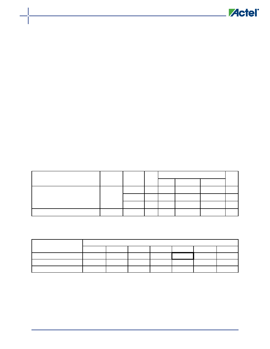
Table 2-5 Package Thermal Resistivities
Package Type
Device
Pin Count
θ
jc
θ
ja
Units
Still Air
200 ft./min.
500 ft./min.
Quad Flat No Lead (QFN)
All devices
48
TBD
C/W
68
TBD
C/W
100
TBD
C/W
Very Thin Quad Flat Pack (VQFP)
All devices
100
10.0
35.3
29.4
27.1
C/W
Table 2-6 Temperature and Voltage Derating Factors for Timing Delays
(normalized to TJ = 70°C, VCC = 1.425 V)
Array Voltage VCC (V)
Junction Temperature (°C)
–40°C
–20°C
0°C
25°C
70°C
85°C
100°C
1.425
0.968
0.973
0.979
0.991
1.000
1.006
1.013
1.500
0.888
0.894
0.899
0.910
0.919
0.924
0.930
1.575
0.836
0.841
0.845
0.856
0.864
0.870
0.875
相关PDF资料 |
PDF描述 |
|---|---|
| A3PN125-2VQG100I | FPGA, 3072 CLBS, 125000 GATES, PQFP100 |
| A3PN125-2VQG100 | FPGA, 3072 CLBS, 125000 GATES, PQFP100 |
| A3PN125-VQ100I | FPGA, 3072 CLBS, 125000 GATES, PQFP100 |
| A3PN125-VQ100 | FPGA, 3072 CLBS, 125000 GATES, PQFP100 |
| A3PN125-VQG100I | FPGA, 3072 CLBS, 125000 GATES, PQFP100 |
相关代理商/技术参数 |
参数描述 |
|---|---|
| A3PN125-2VQ100I | 功能描述:IC FPGA NANO 125K GATES 100-VQFP RoHS:否 类别:集成电路 (IC) >> 嵌入式 - FPGA(现场可编程门阵列) 系列:ProASIC3 nano 标准包装:152 系列:IGLOO PLUS LAB/CLB数:- 逻辑元件/单元数:792 RAM 位总计:- 输入/输出数:120 门数:30000 电源电压:1.14 V ~ 1.575 V 安装类型:表面贴装 工作温度:-40°C ~ 85°C 封装/外壳:289-TFBGA,CSBGA 供应商设备封装:289-CSP(14x14) |
| A3PN125-2VQG100 | 功能描述:IC FPGA NANO 125K GATES 100-VQFP RoHS:是 类别:集成电路 (IC) >> 嵌入式 - FPGA(现场可编程门阵列) 系列:ProASIC3 nano 标准包装:152 系列:IGLOO PLUS LAB/CLB数:- 逻辑元件/单元数:792 RAM 位总计:- 输入/输出数:120 门数:30000 电源电压:1.14 V ~ 1.575 V 安装类型:表面贴装 工作温度:-40°C ~ 85°C 封装/外壳:289-TFBGA,CSBGA 供应商设备封装:289-CSP(14x14) |
| A3PN125-2VQG100I | 功能描述:IC FPGA NANO 125K GATES 100-VQFP RoHS:是 类别:集成电路 (IC) >> 嵌入式 - FPGA(现场可编程门阵列) 系列:ProASIC3 nano 标准包装:152 系列:IGLOO PLUS LAB/CLB数:- 逻辑元件/单元数:792 RAM 位总计:- 输入/输出数:120 门数:30000 电源电压:1.14 V ~ 1.575 V 安装类型:表面贴装 工作温度:-40°C ~ 85°C 封装/外壳:289-TFBGA,CSBGA 供应商设备封装:289-CSP(14x14) |
| A3PN125-DIELOT | 制造商:Microsemi Corporation 功能描述:A3PN125-DIELOT - Gel-pak, waffle pack, wafer, diced wafer on film |
| A3PN125-VQ100 | 功能描述:IC FPGA NANO 125K GATES 100-VQFP RoHS:否 类别:集成电路 (IC) >> 嵌入式 - FPGA(现场可编程门阵列) 系列:ProASIC3 nano 标准包装:152 系列:IGLOO PLUS LAB/CLB数:- 逻辑元件/单元数:792 RAM 位总计:- 输入/输出数:120 门数:30000 电源电压:1.14 V ~ 1.575 V 安装类型:表面贴装 工作温度:-40°C ~ 85°C 封装/外壳:289-TFBGA,CSBGA 供应商设备封装:289-CSP(14x14) |
发布紧急采购,3分钟左右您将得到回复。