- 您现在的位置:买卖IC网 > PDF目录164971 > A3PN125-FVQG100 FPGA, 3072 CLBS, 125000 GATES, PQFP100 PDF资料下载
参数资料
| 型号: | A3PN125-FVQG100 |
| 元件分类: | FPGA |
| 英文描述: | FPGA, 3072 CLBS, 125000 GATES, PQFP100 |
| 封装: | 14 X 14 MM, 1.20 MM HEIGHT, 0.50 MM PITCH, ROHS COMPLIANT, VQFP-100 |
| 文件页数: | 89/92页 |
| 文件大小: | 3184K |
| 代理商: | A3PN125-FVQG100 |
第1页第2页第3页第4页第5页第6页第7页第8页第9页第10页第11页第12页第13页第14页第15页第16页第17页第18页第19页第20页第21页第22页第23页第24页第25页第26页第27页第28页第29页第30页第31页第32页第33页第34页第35页第36页第37页第38页第39页第40页第41页第42页第43页第44页第45页第46页第47页第48页第49页第50页第51页第52页第53页第54页第55页第56页第57页第58页第59页第60页第61页第62页第63页第64页第65页第66页第67页第68页第69页第70页第71页第72页第73页第74页第75页第76页第77页第78页第79页第80页第81页第82页第83页第84页第85页第86页第87页第88页当前第89页第90页第91页第92页
ProASIC3 nano Device Overview
Ad vance v0.4
1-5
The FPGA core consists of a sea of VersaTiles. Each VersaTile can be configured as a three-input
logic function, a D-flip-flop (with or without enable), or a latch by programming the appropriate
flash switch interconnections. The versatility of the ProASIC3 nano core tile as either a three-input
lookup table (LUT) equivalent or as a D-flip-flop/latch with enable allows for efficient use of the
FPGA fabric. The VersaTile capability is unique to the Actel ProASIC3 family of third-generation
architecture flash FPGAs. VersaTiles are connected with any of the four levels of routing hierarchy.
Flash switches are distributed throughout the device to provide nonvolatile, reconfigurable
interconnect programming. Maximum core utilization is possible for virtually any design.
In addition, extensive on-chip programming circuitry allows for rapid, single-voltage (3.3 V)
programming of ProASIC3 nano devices via an IEEE 1532 JTAG interface.
VersaTiles
The ProASIC3 nano core consists of VersaTiles, which have been enhanced beyond the ProASICPLUS
core tiles. The ProASIC3 nano VersaTile supports the following:
All 3-input logic functions—LUT-3 equivalent
Latch with clear or set
D-flip-flop with clear or set
Enable D-flip-flop with clear or set
Refer to Figure 1-5 for VersaTile configurations.
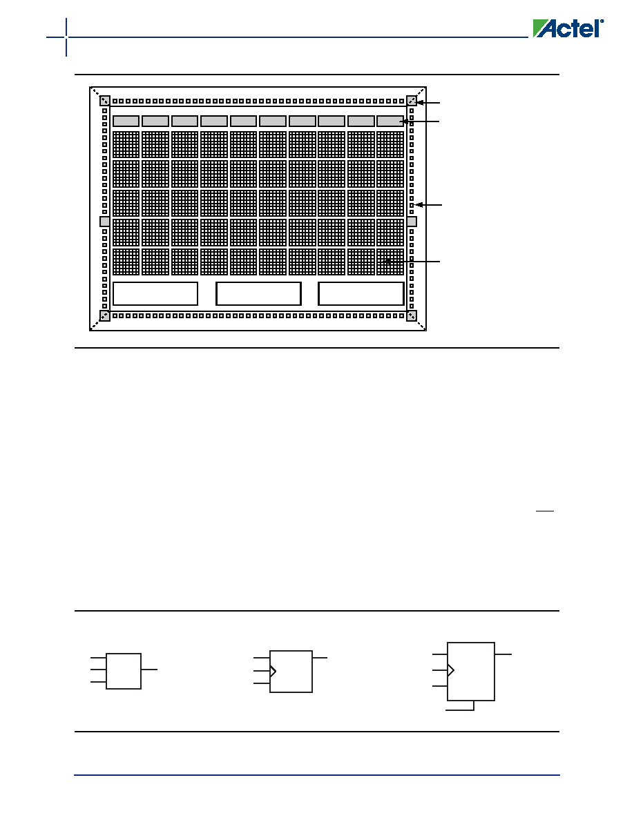
Figure 1-4 ProASIC3 nano Device Architecture Overview with Four I/O Banks (A3PN250)
RAM Block
4,608-Bit Dual-Port
SRAM or FIFO Block
VersaTile
CCC
I/Os
ISP AES
Decryption
User Nonvolatile
FlashROM
Charge Pumps
Bank 0
Bank
3
Bank
3
Bank
1
Bank
1
Bank 2
Figure 1-5 VersaTile Configurations
X1
Y
X2
X3
LUT-3
Data
Y
CLK
Enable
CLR
D-FF
Data
Y
CLK
CLR
D-FF
LUT-3 Equivalent
D-Flip-Flop with Clear or Set
Enable D-Flip-Flop with Clear or Set
相关PDF资料 |
PDF描述 |
|---|---|
| A3PN125-ZFVQ100 | FPGA, 3072 CLBS, 125000 GATES, PQFP100 |
| A3PN125-ZFVQG100 | FPGA, 3072 CLBS, 125000 GATES, PQFP100 |
| A3PN125-1VQ100I | FPGA, 3072 CLBS, 125000 GATES, PQFP100 |
| A3PN125-1VQ100 | FPGA, 3072 CLBS, 125000 GATES, PQFP100 |
| A3PN125-1VQG100I | FPGA, 3072 CLBS, 125000 GATES, PQFP100 |
相关代理商/技术参数 |
参数描述 |
|---|---|
| A3PN125-VQ100 | 功能描述:IC FPGA NANO 125K GATES 100-VQFP RoHS:否 类别:集成电路 (IC) >> 嵌入式 - FPGA(现场可编程门阵列) 系列:ProASIC3 nano 标准包装:152 系列:IGLOO PLUS LAB/CLB数:- 逻辑元件/单元数:792 RAM 位总计:- 输入/输出数:120 门数:30000 电源电压:1.14 V ~ 1.575 V 安装类型:表面贴装 工作温度:-40°C ~ 85°C 封装/外壳:289-TFBGA,CSBGA 供应商设备封装:289-CSP(14x14) |
| A3PN125-VQ100I | 功能描述:IC FPGA NANO 125K GATES 100-VQFP RoHS:否 类别:集成电路 (IC) >> 嵌入式 - FPGA(现场可编程门阵列) 系列:ProASIC3 nano 标准包装:152 系列:IGLOO PLUS LAB/CLB数:- 逻辑元件/单元数:792 RAM 位总计:- 输入/输出数:120 门数:30000 电源电压:1.14 V ~ 1.575 V 安装类型:表面贴装 工作温度:-40°C ~ 85°C 封装/外壳:289-TFBGA,CSBGA 供应商设备封装:289-CSP(14x14) |
| A3PN125-VQG100 | 功能描述:IC FPGA NANO 1024MAC 100VQFP RoHS:是 类别:集成电路 (IC) >> 嵌入式 - FPGA(现场可编程门阵列) 系列:ProASIC3 nano 标准包装:60 系列:XP LAB/CLB数:- 逻辑元件/单元数:10000 RAM 位总计:221184 输入/输出数:244 门数:- 电源电压:1.71 V ~ 3.465 V 安装类型:表面贴装 工作温度:0°C ~ 85°C 封装/外壳:388-BBGA 供应商设备封装:388-FPBGA(23x23) 其它名称:220-1241 |
| A3PN125-VQG100I | 功能描述:IC FPGA NANO 125K GATES 100-VQFP RoHS:是 类别:集成电路 (IC) >> 嵌入式 - FPGA(现场可编程门阵列) 系列:ProASIC3 nano 标准包装:152 系列:IGLOO PLUS LAB/CLB数:- 逻辑元件/单元数:792 RAM 位总计:- 输入/输出数:120 门数:30000 电源电压:1.14 V ~ 1.575 V 安装类型:表面贴装 工作温度:-40°C ~ 85°C 封装/外壳:289-TFBGA,CSBGA 供应商设备封装:289-CSP(14x14) |
| A3PN125-Z1VQ100 | 功能描述:IC FPGA NANO 125K GATES 100-VQFP RoHS:否 类别:集成电路 (IC) >> 嵌入式 - FPGA(现场可编程门阵列) 系列:ProASIC3 nano 标准包装:152 系列:IGLOO PLUS LAB/CLB数:- 逻辑元件/单元数:792 RAM 位总计:- 输入/输出数:120 门数:30000 电源电压:1.14 V ~ 1.575 V 安装类型:表面贴装 工作温度:-40°C ~ 85°C 封装/外壳:289-TFBGA,CSBGA 供应商设备封装:289-CSP(14x14) |
发布紧急采购,3分钟左右您将得到回复。