- 您现在的位置:买卖IC网 > PDF目录164976 > A40MX04-FPL44 FPGA, 547 CLBS, 6000 GATES, 48 MHz, PQCC44 PDF资料下载
参数资料
| 型号: | A40MX04-FPL44 |
| 元件分类: | FPGA |
| 英文描述: | FPGA, 547 CLBS, 6000 GATES, 48 MHz, PQCC44 |
| 封装: | PLASTIC, LCC-44 |
| 文件页数: | 94/124页 |
| 文件大小: | 3142K |
| 代理商: | A40MX04-FPL44 |
第1页第2页第3页第4页第5页第6页第7页第8页第9页第10页第11页第12页第13页第14页第15页第16页第17页第18页第19页第20页第21页第22页第23页第24页第25页第26页第27页第28页第29页第30页第31页第32页第33页第34页第35页第36页第37页第38页第39页第40页第41页第42页第43页第44页第45页第46页第47页第48页第49页第50页第51页第52页第53页第54页第55页第56页第57页第58页第59页第60页第61页第62页第63页第64页第65页第66页第67页第68页第69页第70页第71页第72页第73页第74页第75页第76页第77页第78页第79页第80页第81页第82页第83页第84页第85页第86页第87页第88页第89页第90页第91页第92页第93页当前第94页第95页第96页第97页第98页第99页第100页第101页第102页第103页第104页第105页第106页第107页第108页第109页第110页第111页第112页第113页第114页第115页第116页第117页第118页第119页第120页第121页第122页第123页第124页
40MX and 42MX FPGA Families
v6.1
1-65
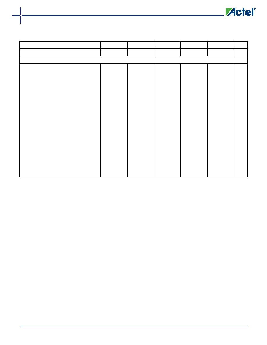
CMOS Output Module Timing5
tDLH
Data-to-Pad HIGH
3.1
3.5
3.9
4.6
6.4
ns
tDHL
Data-to-Pad LOW
2.4
2.6
3.0
3.5
4.9
ns
tENZH
Enable Pad Z to HIGH
2.5
2.8
3.2
3.8
5.3
ns
tENZL
Enable Pad Z to LOW
2.8
3.1
3.5
4.2
5.8
ns
tENHZ
Enable Pad HIGH to Z
5.2
5.7
6.5
7.6
10.7
ns
tENLZ
Enable Pad LOW to Z
4.8
5.3
6.0
7.1
9.9
ns
tGLH
G-to-Pad HIGH
4.9
5.4
6.2
7.2
10.1
ns
tGHL
G-to-Pad LOW
4.9
5.4
6.2
7.2
10.1
ns
tLSU
I/O Latch Set-Up
0.5
0.6
0.7
1.0
ns
tLH
I/O Latch Hold
0.0
ns
tLCO
I/O Latch Clock-to-Out (Pad-to-
Pad) 32 I/O
5.5
6.1
6.9
8.1
11.3
ns
tACO
Array Latch Clock-to-Out (Pad-
to-Pad) 32 I/O
10.6
11.8
13.4
15.7
22.0
ns
dTLH
Capacitive Loading, LOW to HIGH
0.04
0.05
0.07
ns/pF
dTHL
Capacitive Loading, HIGH to LOW
0.03
0.04
0.06
ns/pF
Table 36
A42MX24 Timing Characteristics (Nominal 5.0V Operation) (Continued)
(Worst-Case Commercial Conditions, VCCA = 4.75V, TJ = 70°C)
‘–3’ Speed
‘–2’Speed
‘–1’ Speed
‘Std’ Speed
‘–F’ Speed
Parameter Description
Min.
Max.
Min.
Max.
Min.
Max.
Min.
Max.
Min.
Max. Units
Notes:
1. For dual-module macros, use tPD1 + tRD1 + tPDn, tCO + tRD1 + tPDn, or tPD1 + tRD1 + tSUD, whichever is appropriate.
2. Routing delays are for typical designs across worst-case operating conditions. These parameters should be used for estimating
device performance. Post-route timing analysis or simulation is required to determine actual performance.
3. Data applies to macros based on the S-module. Timing parameters for sequential macros constructed from C-modules can be
obtained from the Timer utility.
4. Set-up and hold timing parameters for the Input Buffer Latch are defined with respect to the PAD and the D input. External setup/
hold timing parameters must account for delay from an external PAD signal to the G inputs. Delay from an external PAD signal to
the G input subtracts (adds) to the internal setup (hold) time.
5. Delays based on 35 pF loading.
相关PDF资料 |
PDF描述 |
|---|---|
| A40MX04-FPL68X79 | FPGA, 547 CLBS, 6000 GATES, 48 MHz, PQCC68 |
| A40MX04-FPL68 | FPGA, 547 CLBS, 6000 GATES, 48 MHz, PQCC68 |
| A40MX04-FPL84X79 | FPGA, 547 CLBS, 6000 GATES, 48 MHz, PQCC84 |
| A40MX04-FPL84 | FPGA, 547 CLBS, 6000 GATES, 48 MHz, PQCC84 |
| A40MX04-FPQ100X79 | FPGA, 547 CLBS, 6000 GATES, 48 MHz, PQFP100 |
相关代理商/技术参数 |
参数描述 |
|---|---|
| A40MX04-FPL44I | 制造商:未知厂家 制造商全称:未知厂家 功能描述:Field Programmable Gate Array (FPGA) |
| A40MX04-FPL44M | 制造商:未知厂家 制造商全称:未知厂家 功能描述:Field Programmable Gate Array (FPGA) |
| A40MX04-FPL68 | 功能描述:IC FPGA MX SGL CHIP 6K 68-PLCC RoHS:否 类别:集成电路 (IC) >> 嵌入式 - FPGA(现场可编程门阵列) 系列:MX 标准包装:152 系列:IGLOO PLUS LAB/CLB数:- 逻辑元件/单元数:792 RAM 位总计:- 输入/输出数:120 门数:30000 电源电压:1.14 V ~ 1.575 V 安装类型:表面贴装 工作温度:-40°C ~ 85°C 封装/外壳:289-TFBGA,CSBGA 供应商设备封装:289-CSP(14x14) |
| A40MX04-FPL68I | 制造商:未知厂家 制造商全称:未知厂家 功能描述:Field Programmable Gate Array (FPGA) |
| A40MX04-FPL68M | 制造商:未知厂家 制造商全称:未知厂家 功能描述:Field Programmable Gate Array (FPGA) |
发布紧急采购,3分钟左右您将得到回复。