- 您现在的位置:买卖IC网 > PDF目录164976 > A40MX04-PL84MX79 FPGA, 547 CLBS, 6000 GATES, 80 MHz, PQCC84 PDF资料下载
参数资料
| 型号: | A40MX04-PL84MX79 |
| 元件分类: | FPGA |
| 英文描述: | FPGA, 547 CLBS, 6000 GATES, 80 MHz, PQCC84 |
| 封装: | PLASTIC, LCC-84 |
| 文件页数: | 33/124页 |
| 文件大小: | 3142K |
| 代理商: | A40MX04-PL84MX79 |
第1页第2页第3页第4页第5页第6页第7页第8页第9页第10页第11页第12页第13页第14页第15页第16页第17页第18页第19页第20页第21页第22页第23页第24页第25页第26页第27页第28页第29页第30页第31页第32页当前第33页第34页第35页第36页第37页第38页第39页第40页第41页第42页第43页第44页第45页第46页第47页第48页第49页第50页第51页第52页第53页第54页第55页第56页第57页第58页第59页第60页第61页第62页第63页第64页第65页第66页第67页第68页第69页第70页第71页第72页第73页第74页第75页第76页第77页第78页第79页第80页第81页第82页第83页第84页第85页第86页第87页第88页第89页第90页第91页第92页第93页第94页第95页第96页第97页第98页第99页第100页第101页第102页第103页第104页第105页第106页第107页第108页第109页第110页第111页第112页第113页第114页第115页第116页第117页第118页第119页第120页第121页第122页第123页第124页
40MX and 42MX FPGA Families
1- 10
v6.1
Design Consideration
It is recommended to use a series 70
Ω termination
resistor on every probe connector (SDI, SDO, MODE,
DCLK, PRA and PRB). The 70
Ω series termination is used
to prevent data transmission corruption during probing
and reading back the checksum.
IEEE Standard 1149.1 Boundary Scan Test
(BST) Circuitry
42MX24 and 42MX36 devices are compatible with IEEE
Standard 1149.1 (informally known as Joint Testing
Action Group Standard or JTAG), which defines a set of
hardware architecture and mechanisms for cost-effective
board-level testing. The basic MX boundary-scan logic
circuit is composed of the TAP (test access port), TAP
controller, test data registers and instruction register
(Figure 1-14 on page 1-11). This circuit supports all
mandatory IEEE 1149.1 instructions (EXTEST, SAMPLE/
PRELOAD and BYPASS) and some optional instructions.
Table 3 on page 1-11 describes the ports that control
JTAG testing, while Table 4 on page 1-11 describes the
test instructions supported by these MX devices.
Each test section is accessed through the TAP, which has
four associated pins: TCK (test clock input), TDI and TDO
(test data input and output), and TMS (test mode
selector).
The TAP controller is a four-bit state machine. The '1's
and '0's represent the values that must be present at TMS
at a rising edge of TCK for the given state transition to
occur. IR and DR indicate that the instruction register or
the data register is operating in that state.
The TAP controller receives two control inputs (TMS and
TCK) and generates control and clock signals for the rest
of the test logic architecture. On power-up, the TAP
controller enters the Test-Logic-Reset state. To guarantee
a reset of the controller from any of the possible states,
TMS must remain high for five TCK cycles.
42MX24 and 42MX36 devices support three types of test
data
registers:
bypass,
device
identification,
and
boundary scan. The bypass register is selected when no
other register needs to be accessed in a device. This
speeds up test data transfer to other devices in a test
data path. The 32-bit device identification register is a
shift register with four fields (lowest significant byte
(LSB), ID number, part number and version). The
boundary-scan register observes and controls the state of
each I/O pin.
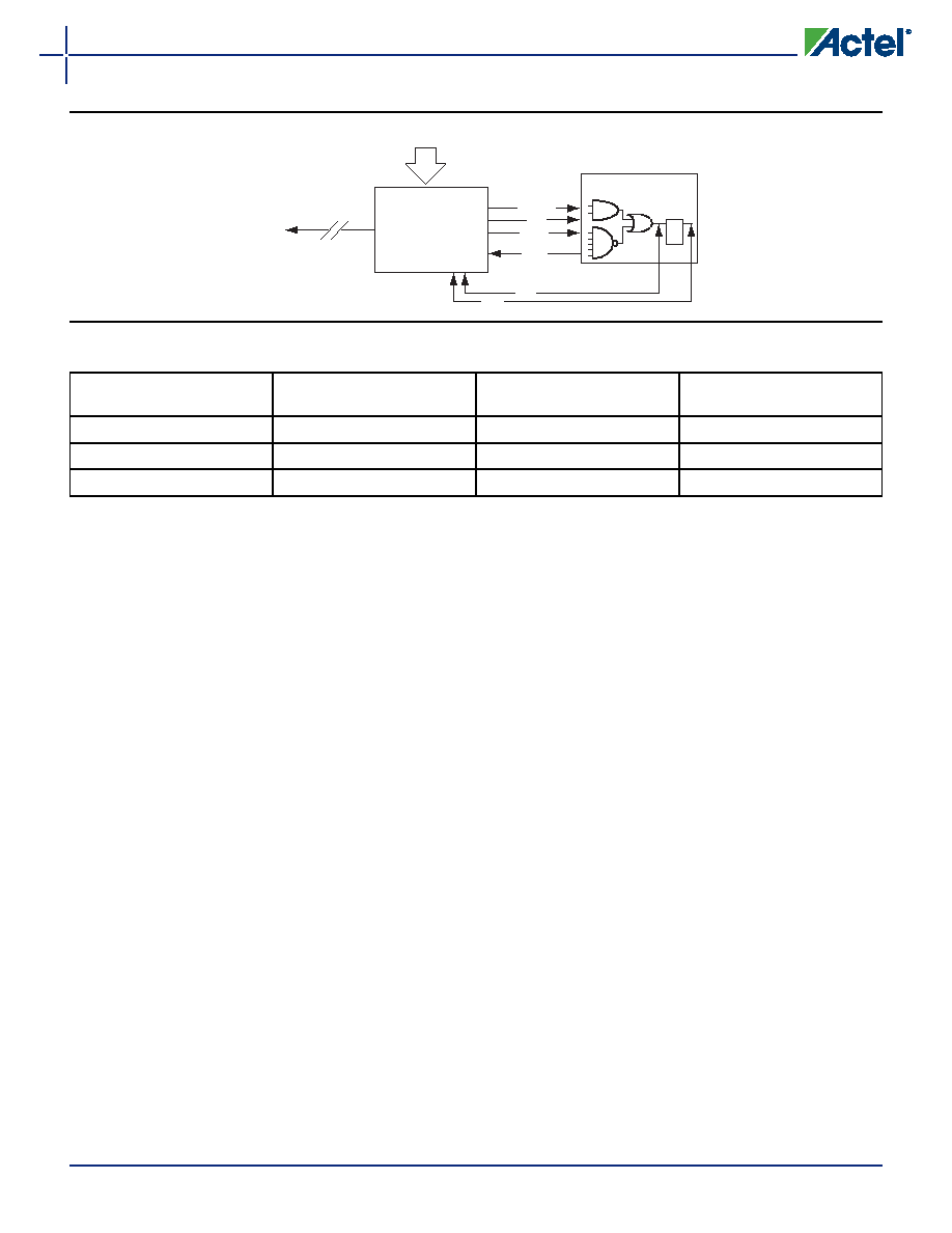
Figure 1-13 Silicon Explorer II Setup with 42MX
Table 2
Device Configuration Options for Probe Capability
Security Fuse(s)
Programmed
MODE
PRA, PRB1
SDI, SDO, DCLK1
No
LOW
User I/Os2
No
HIGH
Probe Circuit Outputs
Probe Circuit Inputs
Yes
–
Probe Circuit Secured
Notes:
1. Avoid using SDI, SDO, DCLK, PRA and PRB pins as input or bidirectional ports. Since these pins are active during probing, input
signals will not pass through these pins and may cause contention.
2. If no user signal is assigned to these pins, they will behave as unused I/Os in this mode. See the <zBlue>“Pin Descriptions” section
on page 77 for information on unused I/O pins.
42MX
Silicon
Explorer II
PRA
PRB
SDO
DCLK
SDI
MODE
Serial Connection
to Windows PC
16 Logic Analyzer Channels
相关PDF资料 |
PDF描述 |
|---|---|
| A40MX04-PL84M | FPGA, 547 CLBS, 6000 GATES, 80 MHz, PQCC84 |
| A40MX04-PL84X79 | FPGA, 547 CLBS, 6000 GATES, 80 MHz, PQCC84 |
| A40MX04-PL84 | FPGA, 547 CLBS, 6000 GATES, 80 MHz, PQCC84 |
| A40MX04-PQ100AX79 | FPGA, 547 CLBS, 6000 GATES, 116 MHz, PQFP100 |
| A40MX04-PQ100A | FPGA, 547 CLBS, 6000 GATES, 116 MHz, PQFP100 |
相关代理商/技术参数 |
参数描述 |
|---|---|
| A40MX04-PLG44 | 功能描述:IC FPGA 69I/O 44PLCC RoHS:是 类别:集成电路 (IC) >> 嵌入式 - FPGA(现场可编程门阵列) 系列:MX 标准包装:24 系列:ECP2 LAB/CLB数:1500 逻辑元件/单元数:12000 RAM 位总计:226304 输入/输出数:131 门数:- 电源电压:1.14 V ~ 1.26 V 安装类型:表面贴装 工作温度:0°C ~ 85°C 封装/外壳:208-BFQFP 供应商设备封装:208-PQFP(28x28) |
| A40MX04-PLG44I | 功能描述:IC FPGA MX SGL CHIP 6K 44-PLCC RoHS:是 类别:集成电路 (IC) >> 嵌入式 - FPGA(现场可编程门阵列) 系列:MX 标准包装:90 系列:ProASIC3 LAB/CLB数:- 逻辑元件/单元数:- RAM 位总计:36864 输入/输出数:157 门数:250000 电源电压:1.425 V ~ 1.575 V 安装类型:表面贴装 工作温度:-40°C ~ 125°C 封装/外壳:256-LBGA 供应商设备封装:256-FPBGA(17x17) |
| A40MX04-PLG44M | 制造商:Microsemi Corporation 功能描述:FPGA 6K GATES 547 CELLS 83MHZ/139MHZ 0.45UM 3.3V/5V 44PLCC - Rail/Tube 制造商:Microsemi Corporation 功能描述:IC FPGA 34 I/O 44PLCC |
| A40MX04-PLG68 | 功能描述:IC FPGA 69I/O 68PLCC RoHS:是 类别:集成电路 (IC) >> 嵌入式 - FPGA(现场可编程门阵列) 系列:MX 标准包装:24 系列:ECP2 LAB/CLB数:1500 逻辑元件/单元数:12000 RAM 位总计:226304 输入/输出数:131 门数:- 电源电压:1.14 V ~ 1.26 V 安装类型:表面贴装 工作温度:0°C ~ 85°C 封装/外壳:208-BFQFP 供应商设备封装:208-PQFP(28x28) |
| A40MX04-PLG68I | 功能描述:IC FPGA MX SGL CHIP 6K 68-PLCC RoHS:是 类别:集成电路 (IC) >> 嵌入式 - FPGA(现场可编程门阵列) 系列:MX 标准包装:90 系列:ProASIC3 LAB/CLB数:- 逻辑元件/单元数:- RAM 位总计:36864 输入/输出数:157 门数:250000 电源电压:1.425 V ~ 1.575 V 安装类型:表面贴装 工作温度:-40°C ~ 125°C 封装/外壳:256-LBGA 供应商设备封装:256-FPBGA(17x17) |
发布紧急采购,3分钟左右您将得到回复。