参数资料
| 型号: | A42MX09-3VQG100I |
| 厂商: | Microsemi SoC |
| 文件页数: | 51/142页 |
| 文件大小: | 0K |
| 描述: | IC FPGA MX SGL CHIP 14K 100VQFP |
| 标准包装: | 90 |
| 系列: | MX |
| 输入/输出数: | 83 |
| 门数: | 14000 |
| 电源电压: | 3 V ~ 3.6 V,4.5 V ~ 5.5 V |
| 安装类型: | 表面贴装 |
| 工作温度: | -40°C ~ 85°C |
| 封装/外壳: | 100-TQFP |
| 供应商设备封装: | 100-VQFP(14x14) |
第1页第2页第3页第4页第5页第6页第7页第8页第9页第10页第11页第12页第13页第14页第15页第16页第17页第18页第19页第20页第21页第22页第23页第24页第25页第26页第27页第28页第29页第30页第31页第32页第33页第34页第35页第36页第37页第38页第39页第40页第41页第42页第43页第44页第45页第46页第47页第48页第49页第50页当前第51页第52页第53页第54页第55页第56页第57页第58页第59页第60页第61页第62页第63页第64页第65页第66页第67页第68页第69页第70页第71页第72页第73页第74页第75页第76页第77页第78页第79页第80页第81页第82页第83页第84页第85页第86页第87页第88页第89页第90页第91页第92页第93页第94页第95页第96页第97页第98页第99页第100页第101页第102页第103页第104页第105页第106页第107页第108页第109页第110页第111页第112页第113页第114页第115页第116页第117页第118页第119页第120页第121页第122页第123页第124页第125页第126页第127页第128页第129页第130页第131页第132页第133页第134页第135页第136页第137页第138页第139页第140页第141页第142页
40MX and 42MX FPGA Families
1- 12
R e v i sio n 1 1
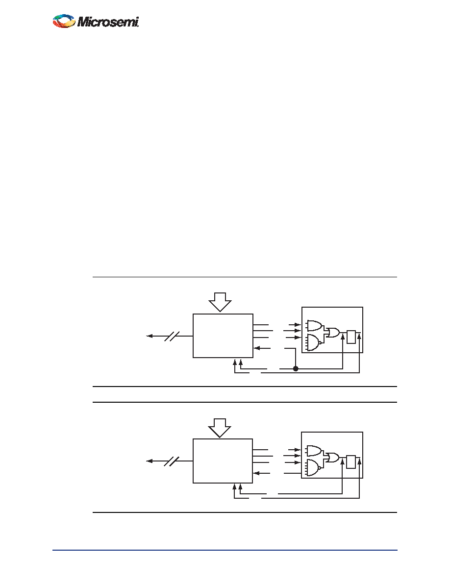
Test Circuitry and Silicon Explorer II Probe
MX devices contain probing circuitry that provides built-in access to every node in a design, via the use of
Silicon Explorer II. Silicon Explorer II is an integrated hardware and software solution that, in conjunction
with the Designer software, allow users to examine any of the internal nets of the device while it is
operating in a prototyping or a production system. The user can probe into an MX device without
changing the placement and routing of the design and without using any additional resources. Silicon
Explorer II's noninvasive method does not alter timing or loading effects, thus shortening the debug cycle
and providing a true representation of the device under actual functional situations.
Silicon Explorer II samples data at 100 MHz (asynchronous) or 66 MHz (synchronous). Silicon Explorer II
attaches to a PC's standard COM port, turning the PC into a fully functional 18-channel logic analyzer.
Silicon Explorer II allows designers to complete the design verification process at their desks and
reduces verification time from several hours per cycle to a few seconds.
Silicon Explorer II is used to control the MODE, DCLK, SDI and SDO pins in MX devices to select the
desired nets for debugging. The user simply assigns the selected internal nets in the Silicon Explorer II
software to the PRA/PRB output pins for observation. Probing functionality is activated when the MODE
pin is held HIGH.
Figure 1-11 illustrates the interconnection between Silicon Explorer II and 40MX devices, while Figure 1-
12 on page 1-12 illustrates the interconnection between Silicon Explorer II and 42MX devices
To allow for probing capabilities, the security fuses must not be programmed. (Refer to "User Security"
section on page 1-8 for the security fuses of 40MX and 42MX devices). Table 1-2 on page 1-13
summarizes the possible device configurations for probing.
PRA and PRB pins are dual-purpose pins. When the "Reserve Probe Pin" is checked in the
Designer software, PRA and PRB pins are reserved as dedicated outputs for probing. If PRA and PRB
pins are required as user I/Os to achieve successful layout and "Reserve Probe Pin" is checked, the
layout tool will override the option and place user I/Os on PRA and PRB pins.
Figure 1-11 Silicon Explorer II Setup with 40MX
Figure 1-12 Silicon Explorer II Setup with 42MX
40MX
Silicon
Explorer II
PRA
PRB
SDO
DCLK
SDI
MODE
Serial Connection
to Windows PC
16 Logic Analyzer Channels
42MX
Silicon
Explorer II
PRA
PRB
SDO
DCLK
SDI
MODE
Serial Connection
to Windows PC
16 Logic Analyzer Channels
相关PDF资料 |
PDF描述 |
|---|---|
| A42MX09-3VQ100I | IC FPGA MX SGL CHIP 14K 100VQFP |
| EPF10K30AQC208-2N | IC FLEX 10KA FPGA 30K 208-PQFP |
| EPF10K30AQC208-2 | IC FLEX 10KA FPGA 30K 208-PQFP |
| EPF10K30ATI144-3N | IC FLEX 10KA FPGA 30K 144-TQFP |
| EPF10K30ATI144-3 | IC FLEX 10KA FPGA 30K 144-TQFP |
相关代理商/技术参数 |
参数描述 |
|---|---|
| A42MX09-BG100 | 制造商:ACTEL 制造商全称:Actel Corporation 功能描述:40MX and 42MX FPGA Families |
| A42MX09-BG100ES | 制造商:ACTEL 制造商全称:Actel Corporation 功能描述:40MX and 42MX FPGA Families |
| A42MX09-BG100I | 制造商:ACTEL 制造商全称:Actel Corporation 功能描述:40MX and 42MX FPGA Families |
| A42MX09-BG100M | 制造商:ACTEL 制造商全称:Actel Corporation 功能描述:40MX and 42MX FPGA Families |
| A42MX09-CQ100 | 制造商:ACTEL 制造商全称:Actel Corporation 功能描述:40MX and 42MX FPGA Families |
发布紧急采购,3分钟左右您将得到回复。