- 您现在的位置:买卖IC网 > PDF目录364584 > a6402 (Altera Corporation) Universal Asynchronous Receiver/Transmitter(通用异步接收/传送器) PDF资料下载
参数资料
| 型号: | a6402 |
| 厂商: | Altera Corporation |
| 英文描述: | Universal Asynchronous Receiver/Transmitter(通用异步接收/传送器) |
| 中文描述: | 通用异步接收器/发送器(通用异步接收/传送器) |
| 文件页数: | 7/8页 |
| 文件大小: | 241K |
| 代理商: | A6402 |
Altera Corporation
63
a6402 Universal Asynchronous Receiver/Transmitter Data Sheet
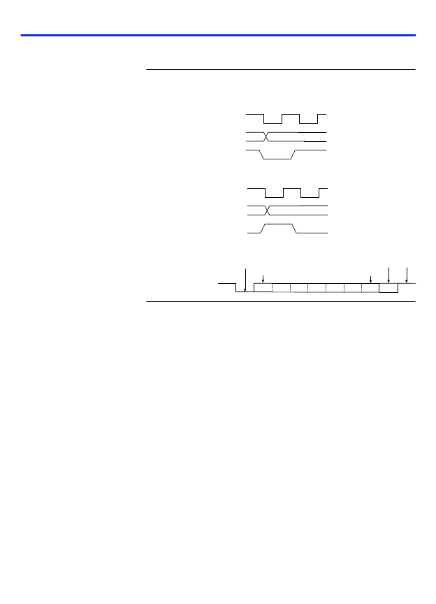
Timing Waveforms
Figure 3
shows the timing waveforms for the
a6402
.
Figure 3. a6402 Functional Timing Waveforms
Variations &
Clarifications
The following characteristics distinguish the Altera
a6402
from the
Harris HD-6402:
I
The
a6402
does not contain the
sfd
and
rrd
inputs, and the
outputs are not tri-stated.
In the
a6402
, the control and transmitter buffer registers are
implemented as registers and use
trc
as a clock source; these
registers are implemented as latches in the HD-6402 device.
In the
a6402
, after
mr
is deasserted, normal operation can
resume on the next
rrc
or
trc
rising clock edge. In the HD-6402
device, normal operation does not resume for 18 clock cycles.
Due to the synchronization process in the
a6402
,
tbre
is
deasserted two clock cycles after the low-to-high transition of
ntbrl
. In the HD-6402 device,
tbre
is deasserted immediately
after the low-to-high transition of
ntbrl
.
In the
a6402
, the
tro
output is registered to remove glitches.
This register uses
trc
as the clock source.
Once the
pe
,
fe
, and
oe
outputs are asserted, the HD-6402
device has no exit condition other than through asserting
mr
.
I
I
I
I
I
Valid Data
trc
cls[2..1], pi
epe, sbs
crl
Control Register Input Cycle
trc
tbr[7..0]
ntbrl
Valid Data
Data Input Cycle
Start Data
LSB
Data
MSB
Parity Stop
tro
Serial Data Format (7 Bits, 1 Parity Bit, 1 Stop Bit)
相关PDF资料 |
PDF描述 |
|---|---|
| A65-1 | Analog IC |
| A655NV400C5 | Interface IC |
| 697NV400C5 | Microprocessor Supervisory Circuits |
| 697NV400M5 | Microprocessor Supervisory Circuits |
| 655NV400C5 | Interface IC |
相关代理商/技术参数 |
参数描述 |
|---|---|
| A6-403-002 | 制造商:Hecon / Danaher 功能描述: |
| A6-40-314-10 | 制造商:Southco 功能描述: |
| A6-404-025 | 制造商:HECON / DANAHER 功能描述: 制造商:Hecon / Danaher 功能描述: |
| A6-404-035 | 制造商:HECON / DANAHER 功能描述: 制造商:Hecon / Danaher 功能描述: |
| A6-404-041 | 制造商:HECON / DANAHER 功能描述: |
发布紧急采购,3分钟左右您将得到回复。