- 您现在的位置:买卖IC网 > PDF目录10031 > AD1555BPZRL (Analog Devices Inc)IC ADC PGA 24BIT LN 28-PLCC PDF资料下载
参数资料
| 型号: | AD1555BPZRL |
| 厂商: | Analog Devices Inc |
| 文件页数: | 14/24页 |
| 文件大小: | 0K |
| 描述: | IC ADC PGA 24BIT LN 28-PLCC |
| 标准包装: | 1 |
| 位数: | 24 |
| 采样率(每秒): | 256k |
| 数据接口: | 串行,并联 |
| 转换器数目: | 1 |
| 功率耗散(最大): | 96mW |
| 电压电源: | 双 ± |
| 工作温度: | -55°C ~ 85°C |
| 安装类型: | 表面贴装 |
| 封装/外壳: | 28-LCC(J 形引线) |
| 供应商设备封装: | 28-PLCC(11.51x11.51) |
| 包装: | 标准包装 |
| 输入数目和类型: | 1 个差分,双极 |
| 其它名称: | AD1555BPZRLDKR |
REV. B
AD1555/AD1556
–21–
AD1556
VL
DGND
DRDY
DRDYBUF = 0
DRDYBUF = 1
TO THE
MICROPROCESSOR
AD1556
VL
DRDY
TO THE
MICROPROCESSOR
TO OTHER
AD1556s
AD1556
VL
DRDY
DGND
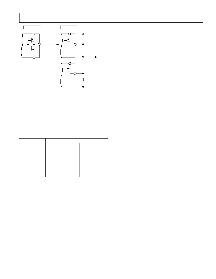
Figure 11. DRDY Output Pin Configuration
Analog Input and Digital Output Data Format
When operating with a nominal MCLK frequency of 256 kHz,
the AD1555 is designed to output a ones-density bitstream from
0.166 to 0.834 on its MDATA output pin corresponding to an
input voltage from –2.25 V to +2.25 V on the MODIN pin.
The AD1556 computes a 24-bit two’s complement output whose
codes range from decimal –6,291,456 to +6,291,455 as shown
in Table VII.
Table VII. Output Coding
Analog Input
Output Code
MODIN
Hexa
Decimal
~ +2.526 V
*
5FFFFF
+6291455
~ +2.25 V
558105
+5603589
~ +2 V
4C00E8
+4980968
~ 0 V
000000
0
~ –2 V
B3FF17
–4980969
~ –2.25 V
AA7EFA
–5603590
~ –2.526 V
*
A00000
–6291456
*Input out of range.
STATUS Register
The AD1556 status register contains 24 bits that capture poten-
tial error conditions and readback the configuration settings.
The status register mapping is defined in Table VIII.
The
ERROR bit is the logical OR of the other error bits, OVWR,
MFLG, and ACC.
ERROR and the other error bits are reset
low after completing a status register read operation or upon
RESET. The
ERROR bit is the inverse of the ERROR output pin.
The OVWR bit indicates if an unread conversion result is over-
written in the output data register. If a data read was started but
not completed when new data is loaded into the output data
register, the OVWR bit is set high.
The MFLG status bit is set to the state of the MFLG input pin
on the rising edge of CLKIN. MFLG will remain set high as long
as the MFLG bit is set. The MFLG status bit will not change
during power-down or RESET.
The ACC bit is set high and the data output is clipped to either
+FS (0111 . . . ) or –FS (1000 . . . ) if an underflow or overflow
has occurred in the digital filter.
The FLSTL bit indicates the digital filter has settled and the
conversion results are an accurate representation of the analog
input. FLSTL is set low on RESET, at power-up, and upon
exiting the power-down state. FLSTL also goes low when SYNC
sets the start of the filter’s convolution cycle, when changes are
made to the device setting with the hardware pins CB0–CB4,
BW0–BW2, or CSEL, and when the MFLG status bit is set
high. When FLSTL is low the OVWR, MFLG, ACC, and DRNG
status bits will not change.
The DRNG bit is used to indicate if the analog input to the
AD1555 is outside its specified operating range. The DRNG bit
is set high whenever the AD1556 digital filter computes four
consecutive output samples that are greater than decimal
+6,291455 or all less than –6,291456.
Layout
The AD1555 has very good immunity to noise on the power
supplies. However, care should still be taken with regard to
grounding layout.
The printed circuit board that houses the AD1555 and the
AD1556 should be designed so the analog and digital sections
are separated and confined to certain areas of the board. This
facilitates the use of ground planes that can be easily separated.
Digital and analog ground planes should be joined in only one
place, preferably underneath the AD1555, or at least as close as
possible to the AD1555. If the AD1555 is in a system where
multiple devices require analog-to-digital ground connections,
the connection should still be made at one point only, a star
ground point, which should be established as close as possible to
the AD1555.
It is recommended to avoid running digital lines under the
device since these will couple noise onto the die. The analog
ground plane should be allowed to run under the AD1555 to
avoid noise coupling. Fast switching signals such as MDATA and
MCLK should be shielded with digital ground to avoid radiating
noise to other sections of the board and should never run near
analog signal paths. Crossover of digital and analog signals
should be avoided. Traces on different but close layers of the
board should run at right angles to each other. This will re-
duce the effect of feedthrough through the board.
The power supply lines to the AD1555 should use as large a
trace as possible to provide low impedance paths and reduce
the effect of glitches on the power supply lines. Good decoupling
is also important to lower the supplies impedance resent to the
AD1555 and reduce the magnitude of the supply spikes. Decou-
pling ceramic capacitors, typically 100 nF, should be placed on
power supply pins +VA, –VA, and VL close to, and ideally right
up against these pins and their corresponding ground pins.
Additionally, low ESR 10
F capacitors should be located in
the vicinity of the ADC to further reduce low frequency ripple.
The VL supply of the AD1555 can either be a separate supply
or come from the analog supply VA. When the system digital
supply is noisy, or fast switching digital signals are present, it is
recommended, if no separate supply is available, to connect the
VL digital supply to the analog supply VA through an RC filter
as shown in Figure 7.
相关PDF资料 |
PDF描述 |
|---|---|
| VI-26M-MX-F1 | CONVERTER MOD DC/DC 10V 75W |
| AD678AJ | IC ADC 12BIT 200KSPS 44-JLCC |
| IDT72V3611L15PF8 | IC FIFO SYNC 64X36 15NS 120-TQFP |
| MS27468T21A16P | CONN RCPT 16POS JAM NUT W/PINS |
| MS27468E21A16P | CONN RCPT 16POS JAM NUT W/PINS |
相关代理商/技术参数 |
参数描述 |
|---|---|
| AD1556 | 制造商:AD 制造商全称:Analog Devices 功能描述:24-Bit ADC WITH LOW NOISE PGA |
| AD1556AS | 制造商:Analog Devices 功能描述:ADC Single Delta-Sigma 256ksps 24-bit Parallel/Serial 44-Pin MQFP 制造商:Rochester Electronics LLC 功能描述:- Bulk |
| AD1556ASRL | 制造商:Analog Devices 功能描述:ADC Single Delta-Sigma 256ksps 24-bit Parallel/Serial 44-Pin MQFP T/R |
| AD1556ASZ | 功能描述:IC ADC PGA 24BIT LN 44MQFP RoHS:是 类别:集成电路 (IC) >> 数据采集 - 模数转换器 系列:- 其它有关文件:TSA1204 View All Specifications 标准包装:1 系列:- 位数:12 采样率(每秒):20M 数据接口:并联 转换器数目:2 功率耗散(最大):155mW 电压电源:模拟和数字 工作温度:-40°C ~ 85°C 安装类型:表面贴装 封装/外壳:48-TQFP 供应商设备封装:48-TQFP(7x7) 包装:Digi-Reel® 输入数目和类型:4 个单端,单极;2 个差分,单极 产品目录页面:1156 (CN2011-ZH PDF) 其它名称:497-5435-6 |
| AD1556ASZRL | 制造商:Analog Devices 功能描述:ADC Single Delta-Sigma 256ksps 24-bit Parallel/Serial 44-Pin MQFP T/R |
发布紧急采购,3分钟左右您将得到回复。