- 您现在的位置:买卖IC网 > PDF目录10038 > AD1671JQ (Analog Devices Inc)IC ADC SNGL 12BIT 28-CDIP PDF资料下载
参数资料
| 型号: | AD1671JQ |
| 厂商: | Analog Devices Inc |
| 文件页数: | 1/16页 |
| 文件大小: | 0K |
| 描述: | IC ADC SNGL 12BIT 28-CDIP |
| 标准包装: | 1 |
| 位数: | 12 |
| 采样率(每秒): | 1.25M |
| 数据接口: | 并联 |
| 转换器数目: | 2 |
| 功率耗散(最大): | 750mW |
| 电压电源: | 模拟和数字,双 ± |
| 工作温度: | 0°C ~ 70°C |
| 安装类型: | 通孔 |
| 封装/外壳: | 28-CDIP(0.600",15.24mm) |
| 供应商设备封装: | 28-CDIP |
| 包装: | 管件 |
| 输入数目和类型: | 2 个单端,双极;2 个单端,单极 |
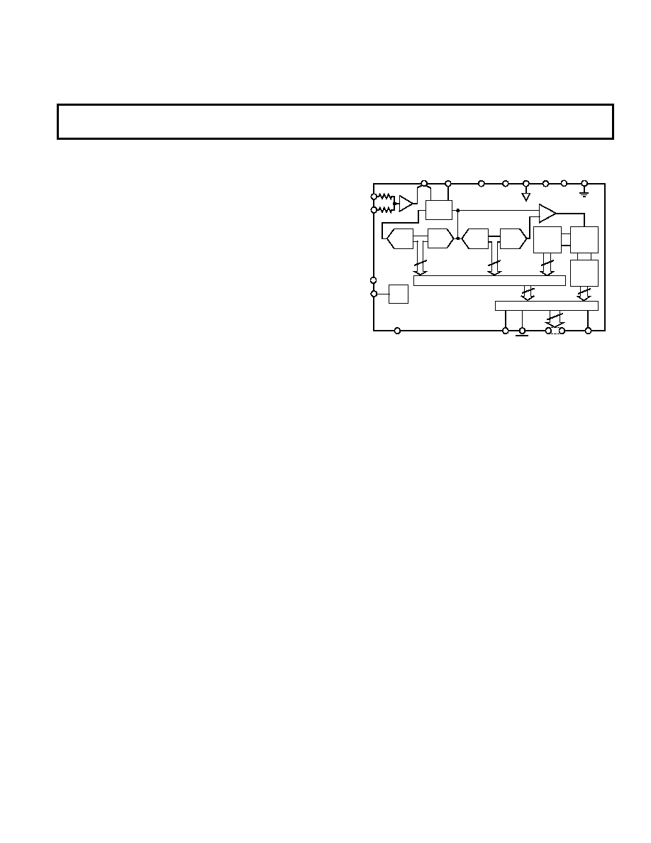
FUNCTIONAL BLOCK DIAGRAM
UPO/BPO
ENCODE
OTR
SHA
OUT
AIN1
S/H
2.5V
REF
REF OUT
REF IN
LATCHES
CORRECTION LOGIC
8-BIT
LADDER
MATRIX
AD1671
3
3-BIT
FLASH
REF COM
AIN2
5k
VCC
ACOM
V
EE
V
LOGIC
DCOM
3-BIT
FLASH
DAC
FINE
4-BIT
FLASH
COARSE
4-BIT
FLASH
4
DAC
3
12
MSB
DAV
BIT 1 –12
4
8
X4
RANGE
SELECT
REV. B
Information furnished by Analog Devices is believed to be accurate and
reliable. However, no responsibility is assumed by Analog Devices for its
use, nor for any infringements of patents or other rights of third parties
which may result from its use. No license is granted by implication or
otherwise under any patent or patent rights of Analog Devices.
a
Complete 12-Bit 1.25 MSPS
Monolithic A/D Converter
AD1671
One Technology Way, P.O. Box 9106, Norwood, MA 02062-9106, U.S.A.
Tel: 617/329-4700
Fax: 617/326-8703
FEATURES
Conversion Time: 800 ns
1.25 MHz Throughput Rate
Complete: On-Chip Sample-and-Hold Amplifier and
Voltage Reference
Low Power Dissipation: 570 mW
No Missing Codes Guaranteed
Signal-to-Noise Plus Distortion Ratio
fIN = 100 kHz: 70 dB
Pin Configurable Input Voltage Ranges
Twos Complement or Offset Binary Output Data
28-Pin DIP and 28-Pin Surface Mount Package
Out of Range Indicator
PRODUCT DESCRIPTION
The AD1671 is a monolithic 12-bit, 1.25 MSPS analog-to-
digital converter with an on-board, high performance sample-
and-hold amplifier (SHA) and voltage reference. The AD1671
guarantees no missing codes over the full operating tempera-
ture range. The combination of a merged high speed bipolar/
CMOS process and a novel architecture results in a combi-
nation of speed and power consumption far superior to pre-
viously available hybrid implementations. Additionally, the
greater reliability of monolithic construction offers improved
system reliability and lower costs than hybrid designs.
The fast settling input SHA is equally suited for both multi-
plexed systems that switch negative to positive full-scale
voltage levels in successive channels and sampling inputs at
frequencies up to and beyond the Nyquist rate. The AD1671
provides both reference output and reference input pins, al-
lowing the on-board reference to serve as a system reference.
An external reference can also be chosen to suit the dc accu-
racy and temperature drift requirements of the application.
The AD1671 uses a subranging flash conversion technique,
with digital error correction for possible errors introduced in
the first part of the conversion cycle. An on-chip timing gen-
erator provides strobe pulses for each of the four internal
flash cycles. A single ENCODE pulse is used to control the
converter. The digital output data is presented in twos
complement or offset binary output format. An out-of-range
signal indicates an overflow condition. It can be used with
the most significant bit to determine low or high overflow.
The performance of the AD1671 is made possible by using high
speed, low noise bipolar circuitry in the linear sections and low
power CMOS for the logic sections. Analog Devices’ ABCMOS-1
process provides both high speed bipolar and 2-micron CMOS
devices on a single chip. Laser trimmed thin-film resistors are
used to provide accuracy and temperature stability.
The AD1671 is available in two performance grades and three
temperature ranges. The AD1671J and K grades are available
over the 0
°C to +70°C temperature range. The AD1671A grade
is available over the –40
°C to +85°C temperature range. The
AD1671S grade is available over the –55
°C to +125°C tempera-
ture range.
PRODUCT HIGHLIGHTS
The AD1671 offers a complete single chip sampling 12-bit,
1.25 MSPS analog-to-digital conversion function in a 28-pin
package.
The AD1671 at 570 mW consumes a fraction of the power of
currently available hybrids.
An OUT OF RANGE output bit indicates when the input sig-
nal is beyond the AD1671’s input range.
Input signal ranges are 0 V to +5 V unipolar or
±5 V bipolar,
selected by pin strapping, with an input resistance of 10 k
.
The input signal range can also be pin strapped for 0 V to +2.5 V
unipolar or
±2.5 V bipolar with an input resistance of 10 M.
Output data is available in unipolar, bipolar offset or bipolar
twos complement binary format.
相关PDF资料 |
PDF描述 |
|---|---|
| VI-BNP-IV-F1 | CONVERTER MOD DC/DC 13.8V 150W |
| VE-J60-MW-B1 | CONVERTER MOD DC/DC 5V 100W |
| AD7878LPZ | IC ADC 12BIT W/DSP INT 28-PLCC |
| VI-BNN-IV-F4 | CONVERTER MOD DC/DC 18.5V 150W |
| MS27473T10F35PA | CONN PLUG 13POS STRAIGHT W/PINS |
相关代理商/技术参数 |
参数描述 |
|---|---|
| AD1671K | 制造商:AD 制造商全称:Analog Devices 功能描述:Complete 12-Bit 1.25 MSPS Monolithic A/D Converter |
| AD1671KP | 功能描述:IC ADC SNGL 12BIT 28PLCC RoHS:否 类别:集成电路 (IC) >> 数据采集 - 模数转换器 系列:- 产品培训模块:Lead (SnPb) Finish for COTS Obsolescence Mitigation Program 标准包装:250 系列:- 位数:12 采样率(每秒):1.8M 数据接口:并联 转换器数目:1 功率耗散(最大):1.82W 电压电源:模拟和数字 工作温度:-40°C ~ 85°C 安装类型:表面贴装 封装/外壳:48-LQFP 供应商设备封装:48-LQFP(7x7) 包装:管件 输入数目和类型:2 个单端,单极 |
| AD1671KPZ | 制造商:Analog Devices 功能描述:ADC Single Pipelined 1.25Msps 12-bit Parallel 28-Pin PLCC 制造商:Analog Devices 功能描述:IC, 12-BIT 1.25 MSPS ADC - Rail/Tube |
| AD1671KQ | 功能描述:IC ADC SNGL 12BIT 28-CDIP RoHS:否 类别:集成电路 (IC) >> 数据采集 - 模数转换器 系列:- 产品培训模块:Lead (SnPb) Finish for COTS Obsolescence Mitigation Program 标准包装:250 系列:- 位数:12 采样率(每秒):1.8M 数据接口:并联 转换器数目:1 功率耗散(最大):1.82W 电压电源:模拟和数字 工作温度:-40°C ~ 85°C 安装类型:表面贴装 封装/外壳:48-LQFP 供应商设备封装:48-LQFP(7x7) 包装:管件 输入数目和类型:2 个单端,单极 |
| AD1671S | 制造商:AD 制造商全称:Analog Devices 功能描述:Complete 12-Bit 1.25 MSPS Monolithic A/D Converter |
发布紧急采购,3分钟左右您将得到回复。