- 您现在的位置:买卖IC网 > PDF目录10038 > AD1671JQ (Analog Devices Inc)IC ADC SNGL 12BIT 28-CDIP PDF资料下载
参数资料
| 型号: | AD1671JQ |
| 厂商: | Analog Devices Inc |
| 文件页数: | 11/16页 |
| 文件大小: | 0K |
| 描述: | IC ADC SNGL 12BIT 28-CDIP |
| 标准包装: | 1 |
| 位数: | 12 |
| 采样率(每秒): | 1.25M |
| 数据接口: | 并联 |
| 转换器数目: | 2 |
| 功率耗散(最大): | 750mW |
| 电压电源: | 模拟和数字,双 ± |
| 工作温度: | 0°C ~ 70°C |
| 安装类型: | 通孔 |
| 封装/外壳: | 28-CDIP(0.600",15.24mm) |
| 供应商设备封装: | 28-CDIP |
| 包装: | 管件 |
| 输入数目和类型: | 2 个单端,双极;2 个单端,单极 |
AD1671
REV. B
–4–
PIN DESCRIPTION
Symbol
Pin No.
Type
Name and Function
ACOM
27
P
Analog Ground.
AIN
22, 23
AI
Analog Inputs, AIN1 and AIN2. The AD1671 can be pin strapped for four input ranges:
Range
Pin Strap
Signal Input
0 to +2.5 V,
±2.5 V
Connect AIN1 to AIN2
AIN1 or AIN2
0 to +5 V,
±5 V
Connect AIN1 or AIN2 to ACOM
AIN1 or AIN2
BIT 1 (MSB)
13
DO
Most Significant Bit.
BIT 2–BIT 11
12-3
DO
Data Bits 2 through 11.
BIT 12 (LSB)
2
DO
Least Significant Bit.
BPO/UPO
26
AI
Bipolar or Unipolar Configuration Pin. See section on Input Range Connections for details.
DAV
16
DO
Data Available Output. The rising edge of DAV indicates an end of conversion and can be used
to latch current data into an external register. The falling edge of DAV can be used to latch
previous dam into an external register.
DCOM
19
P
Digital Ground.
ENCODE
17
DI
The analog input is sampled on the rising edge of ENCODE.
MSB
14
DO
Inverted Most Significant Bit. Provides twos complement output data format.
OTR
15
DO
Out of Range is Active HIGH when the analog input is out of range. See Output Data Format,
Table III.
REF COM
20
AI
REF COM is the internal reference ground pin. REF COM should be connected as indicated
in the Grounding and Decoupling Rules and Optional External Reference Connection Sections.
REF IN
24
AI
REF IN is the external 2.5 V reference input.
REF OUT
21
AO
REF OUT is the internal 2.5 V reference output.
SHA OUT
25
AO
No Connect for bipolar input ranges. Connect SHA OUT to BPO/UPO for unipolar input ranges.
VCC
28
P
+5 V Analog Power.
VEE
1
P
–5 V Analog Power.
VLOGIC
18
P
+5 V Digital Power.
TYPE: AI = Analog Input; AO = Analog Output; DI = Digital Input; DO = Digital Outputs; P = Power.
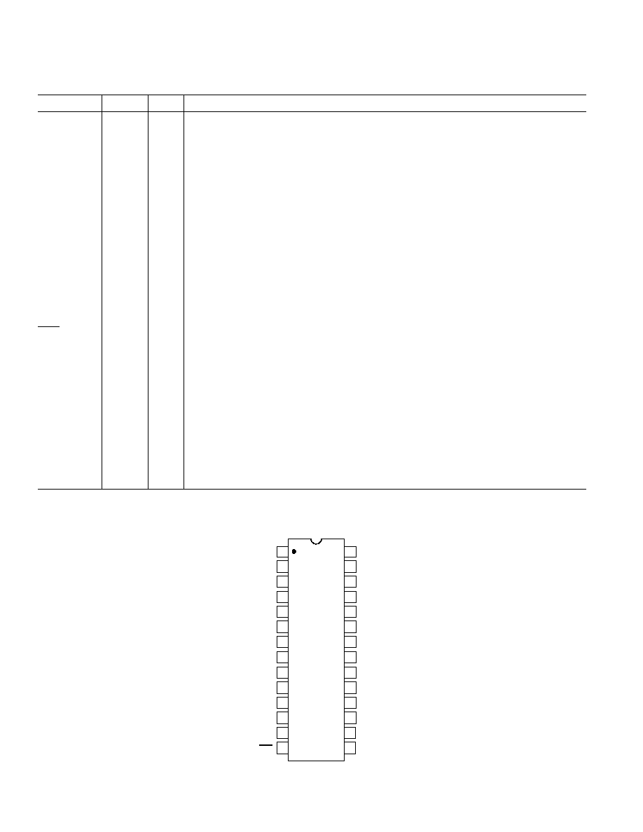
PIN CONFIGURATION
ACOM
BPO/UPO
DCOM
ENCODE
DAV
OTR
MSB
BIT 12 (LSB)
BIT 11
BIT 10
BIT 9
BIT 8
BIT 7
BIT 6
BIT 5
BIT 4
BIT 3
BIT 2
BIT 1 (MSB)
AIN1
REF COM
REF OUT
AIN2
SHA OUT
1
2
3
7
28
27
26
22
8
9
10
21
20
19
11
12
18
17
4
5
25
24
6
23
TOP VIEW
(Not to Scale)
13
14
16
15
AD1671
VEE
VCC
V
LOGIC
REF IN
相关PDF资料 |
PDF描述 |
|---|---|
| VI-BNP-IV-F1 | CONVERTER MOD DC/DC 13.8V 150W |
| VE-J60-MW-B1 | CONVERTER MOD DC/DC 5V 100W |
| AD7878LPZ | IC ADC 12BIT W/DSP INT 28-PLCC |
| VI-BNN-IV-F4 | CONVERTER MOD DC/DC 18.5V 150W |
| MS27473T10F35PA | CONN PLUG 13POS STRAIGHT W/PINS |
相关代理商/技术参数 |
参数描述 |
|---|---|
| AD1671K | 制造商:AD 制造商全称:Analog Devices 功能描述:Complete 12-Bit 1.25 MSPS Monolithic A/D Converter |
| AD1671KP | 功能描述:IC ADC SNGL 12BIT 28PLCC RoHS:否 类别:集成电路 (IC) >> 数据采集 - 模数转换器 系列:- 产品培训模块:Lead (SnPb) Finish for COTS Obsolescence Mitigation Program 标准包装:250 系列:- 位数:12 采样率(每秒):1.8M 数据接口:并联 转换器数目:1 功率耗散(最大):1.82W 电压电源:模拟和数字 工作温度:-40°C ~ 85°C 安装类型:表面贴装 封装/外壳:48-LQFP 供应商设备封装:48-LQFP(7x7) 包装:管件 输入数目和类型:2 个单端,单极 |
| AD1671KPZ | 制造商:Analog Devices 功能描述:ADC Single Pipelined 1.25Msps 12-bit Parallel 28-Pin PLCC 制造商:Analog Devices 功能描述:IC, 12-BIT 1.25 MSPS ADC - Rail/Tube |
| AD1671KQ | 功能描述:IC ADC SNGL 12BIT 28-CDIP RoHS:否 类别:集成电路 (IC) >> 数据采集 - 模数转换器 系列:- 产品培训模块:Lead (SnPb) Finish for COTS Obsolescence Mitigation Program 标准包装:250 系列:- 位数:12 采样率(每秒):1.8M 数据接口:并联 转换器数目:1 功率耗散(最大):1.82W 电压电源:模拟和数字 工作温度:-40°C ~ 85°C 安装类型:表面贴装 封装/外壳:48-LQFP 供应商设备封装:48-LQFP(7x7) 包装:管件 输入数目和类型:2 个单端,单极 |
| AD1671S | 制造商:AD 制造商全称:Analog Devices 功能描述:Complete 12-Bit 1.25 MSPS Monolithic A/D Converter |
发布紧急采购,3分钟左右您将得到回复。