- 您现在的位置:买卖IC网 > PDF目录10038 > AD1671JQ (Analog Devices Inc)IC ADC SNGL 12BIT 28-CDIP PDF资料下载
参数资料
| 型号: | AD1671JQ |
| 厂商: | Analog Devices Inc |
| 文件页数: | 2/16页 |
| 文件大小: | 0K |
| 描述: | IC ADC SNGL 12BIT 28-CDIP |
| 标准包装: | 1 |
| 位数: | 12 |
| 采样率(每秒): | 1.25M |
| 数据接口: | 并联 |
| 转换器数目: | 2 |
| 功率耗散(最大): | 750mW |
| 电压电源: | 模拟和数字,双 ± |
| 工作温度: | 0°C ~ 70°C |
| 安装类型: | 通孔 |
| 封装/外壳: | 28-CDIP(0.600",15.24mm) |
| 供应商设备封装: | 28-CDIP |
| 包装: | 管件 |
| 输入数目和类型: | 2 个单端,双极;2 个单端,单极 |
AD1671
REV. B
–10–
UNIPOLAR (0 V TO +2.5 V) CALIBRATION
The connections for the 0 V to +2.5 V input range calibration is
shown in Figure 11. Figure 11 shows an example of how the
offset error can be trimmed in front of the AD1671. The proce-
dure for trimming the offset and gain errors is the same as for
the unipolar 5 V range.
AIN1
AIN2
5k
SHA OUT
BPO/UPO
AD1671
REF IN
REF OUT
SHA
OFFSET ADJ
+15V
1k
0 TO +2.5V
VIN
10k
R2
2k
GAIN
ADJ
1F
R1
AD845
1k
390
Figure 11. Unipolar (0 V to +2.5 V) Calibration
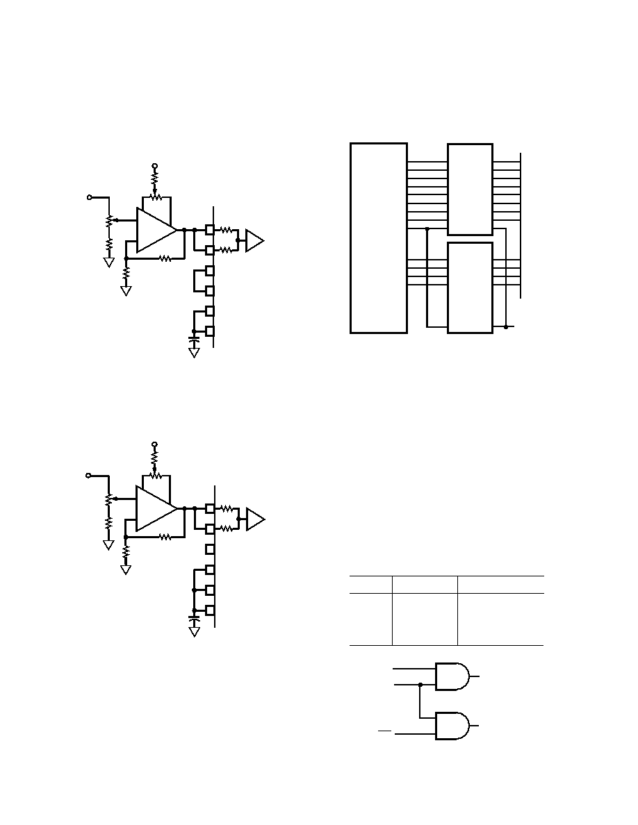
BIPOLAR ( 2.5 V) CALIBRATION
The connections for the bipolar
±2.5 V input range is shown in
Figure 12.
AIN1
AIN2
5k
SHA OUT
BPO/UPO
AD1671
REF IN
REF OUT
SHA
OFFSET ADJ
+15V
1k
VIN
10k
R2
2k
GAIN
ADJ
1F
R1
AD845
1k
390
–2.5V TO +2.5V
Figure 12. Bipolar (
±2.5 V) Calibration
OUTPUT LATCHES
Figure 13 shows the AD1671 connected to the 74HC574 octal
D-type edge-triggered latches with 3-state outputs. The latch
can drive highly capacitive loads (i.e., bus lines, I/O ports) while
maintaining the data signal integrity. The maximum setup and
hold times of the 574 type latch must be less than 20 ns (tDD
and tSS minimum). To satisfy the requirements of the 574 type
latch the recommended logic families are S, AS, ALS, F or
BCT. New data from the AD1671 is latched on the rising edge
of the DAV (Pin 16) output pulse. Previous data can be latched
by inverting the DAV output with a 7404 type inverter.
BIT 1
BIT 2
BIT 3
BIT 4
BIT 5
BIT 6
BIT 7
BIT 8
BIT 9
BIT 10
BIT 11
BIT 12
DAV
DATA BUS
3-STATE
CONTROL
AD1671
1D
2D
3D
4D
5D
6D
7D
8D
CLOCK
1Q
2Q
3Q
4Q
5Q
6Q
7Q
8Q
74HC574
OC
1D
2D
3D
4D
5D
6D
7D
8D
CLOCK
1Q
2Q
3Q
4Q
5Q
6Q
7Q
8Q
74HC574
OC
Figure 13. AD1671 to Output Latches
OUT OF RANGE
An out-of-range condition exists when the analog input voltage
is beyond the input range (0 V to +2.5 V, 0 V to +5 V,
±2.5 V,
±5 V) of the converter OTR (Pin 15) is set low when the analog
input voltage is within the analog input range. OTR is set HIGH
and will remain HIGH when the analog input voltage exceeds
the input range by typically 1/2 LSB (OTR transition is tested to
±6 LSBs of accuracy) from the center of the ±full-scale output
codes. OTR will remain HIGH until the analog input is within
the input range and another conversion is completed. By logical
ANDing OTR with the MSB and its complement, overrange
high or underrange low conditions can be detected. Table II is a
truth table for the over/under range circuit in Figure 14. Sys-
tems requiring programmable gain conditioning prior to the
AD1671 can immediately detect an out-of-range condition, thus
eliminating gain selection iterations.
Table II. Out-of-Range Truth Table
OTR
MSB
Analog Input Is
0
In Range
0
1
In Range
1
0
Underrange
1
Overrange
MSB
OTR
MSB
OVER = "1"
UNDER = "1"
Figure 14. Overrange or Underrange Logic
相关PDF资料 |
PDF描述 |
|---|---|
| VI-BNP-IV-F1 | CONVERTER MOD DC/DC 13.8V 150W |
| VE-J60-MW-B1 | CONVERTER MOD DC/DC 5V 100W |
| AD7878LPZ | IC ADC 12BIT W/DSP INT 28-PLCC |
| VI-BNN-IV-F4 | CONVERTER MOD DC/DC 18.5V 150W |
| MS27473T10F35PA | CONN PLUG 13POS STRAIGHT W/PINS |
相关代理商/技术参数 |
参数描述 |
|---|---|
| AD1671K | 制造商:AD 制造商全称:Analog Devices 功能描述:Complete 12-Bit 1.25 MSPS Monolithic A/D Converter |
| AD1671KP | 功能描述:IC ADC SNGL 12BIT 28PLCC RoHS:否 类别:集成电路 (IC) >> 数据采集 - 模数转换器 系列:- 产品培训模块:Lead (SnPb) Finish for COTS Obsolescence Mitigation Program 标准包装:250 系列:- 位数:12 采样率(每秒):1.8M 数据接口:并联 转换器数目:1 功率耗散(最大):1.82W 电压电源:模拟和数字 工作温度:-40°C ~ 85°C 安装类型:表面贴装 封装/外壳:48-LQFP 供应商设备封装:48-LQFP(7x7) 包装:管件 输入数目和类型:2 个单端,单极 |
| AD1671KPZ | 制造商:Analog Devices 功能描述:ADC Single Pipelined 1.25Msps 12-bit Parallel 28-Pin PLCC 制造商:Analog Devices 功能描述:IC, 12-BIT 1.25 MSPS ADC - Rail/Tube |
| AD1671KQ | 功能描述:IC ADC SNGL 12BIT 28-CDIP RoHS:否 类别:集成电路 (IC) >> 数据采集 - 模数转换器 系列:- 产品培训模块:Lead (SnPb) Finish for COTS Obsolescence Mitigation Program 标准包装:250 系列:- 位数:12 采样率(每秒):1.8M 数据接口:并联 转换器数目:1 功率耗散(最大):1.82W 电压电源:模拟和数字 工作温度:-40°C ~ 85°C 安装类型:表面贴装 封装/外壳:48-LQFP 供应商设备封装:48-LQFP(7x7) 包装:管件 输入数目和类型:2 个单端,单极 |
| AD1671S | 制造商:AD 制造商全称:Analog Devices 功能描述:Complete 12-Bit 1.25 MSPS Monolithic A/D Converter |
发布紧急采购,3分钟左右您将得到回复。