- 您现在的位置:买卖IC网 > PDF目录10938 > AD1838AASZ-REEL (Analog Devices Inc)IC CODEC 2ADC/6DAC 24 BIT 52MQFP PDF资料下载
参数资料
| 型号: | AD1838AASZ-REEL |
| 厂商: | Analog Devices Inc |
| 文件页数: | 4/24页 |
| 文件大小: | 0K |
| 描述: | IC CODEC 2ADC/6DAC 24 BIT 52MQFP |
| 标准包装: | 800 |
| 类型: | 立体声音频 |
| 数据接口: | 串行 |
| 分辨率(位): | 24 b |
| ADC / DAC 数量: | 2 / 6 |
| 三角积分调变: | 是 |
| S/N 比,标准 ADC / DAC (db): | 105 / 108 |
| 动态范围,标准 ADC / DAC (db): | 105 / 108 |
| 电压 - 电源,模拟: | 4.5 V ~ 5.5 V |
| 电压 - 电源,数字: | 4.5 V ~ 5.5 V |
| 工作温度: | -40°C ~ 85°C |
| 安装类型: | 表面贴装 |
| 封装/外壳: | 52-QFP |
| 供应商设备封装: | 52-MQFP(10x10) |
| 包装: | 带卷 (TR) |
REV. A
AD1838A
–12–
RESET and Power-Down
PD/RST powers down the chip and sets the control registers to
their default settings. After
PD/RST is de-asserted, an initializa-
tion routine runs inside the AD1838A to clear all memories to
zero. This initialization lasts for approximately 20 LRCLK
intervals. During this time, it is recommended that no SPI
writes occur.
Power Supply and Voltage Reference
The AD1838A is designed for 5 V supplies. Separate power supply
pins are provided for the analog and digital sections. These pins
should be bypassed with 100 nF ceramic chip capacitors, as
close to the pins as possible, to minimize noise pickup. A bulk
aluminum electrolytic capacitor of at least 22
F should also be
provided on the same PC board as the codec. For critical appli-
cations, improved performance will be obtained with separate
supplies for the analog and digital sections. If this is not possible, it
is recommended that the analog and digital supplies be isolated by
two ferrite beads in series with the bypass capacitor of each supply.
It is important that the analog supply be as clean as possible.
The internal voltage reference is brought out on the FILTR pin
and should be bypassed as close as possible to the chip, with a
parallel combination of 10
F and 100 nF. The reference volt-
age may be used to bias external op amps to the common-mode
voltage of the analog input and output signal pins. The current
drawn from the FILTR pin should be limited to less than 50
A.
Serial Control Port
The AD1838A has an SPI compatible control port to permit
programming the internal control registers for the ADCs and
DACs and to read the ADC signal levels from the internal peak
detectors. The SPI control port is a 4-wire serial control port. The
format is similar to the Motorola SPI format except the
input data-word is 16 bits wide. The maximum serial bit clock
frequency is 12.5 MHz and may be completely asynchronous to the
sample rate of the ADCs and DACs. Figure 3 shows the format
of the SPI signal.
Serial Data Ports—Data Format
The ADC serial data output mode defaults to the popular I
2S
format, where the data is delayed by one BCLK interval from
the edge of the LRCLK. By changing Bits 6 to 8 in ADC Con-
trol Register 2, the serial mode can be changed to right-justified
(RJ), left-justified DSP (DSP), or left-justified (LJ). In the RJ
mode, it is necessary to set Bits 4 and 5 to define the width of
the data-word.
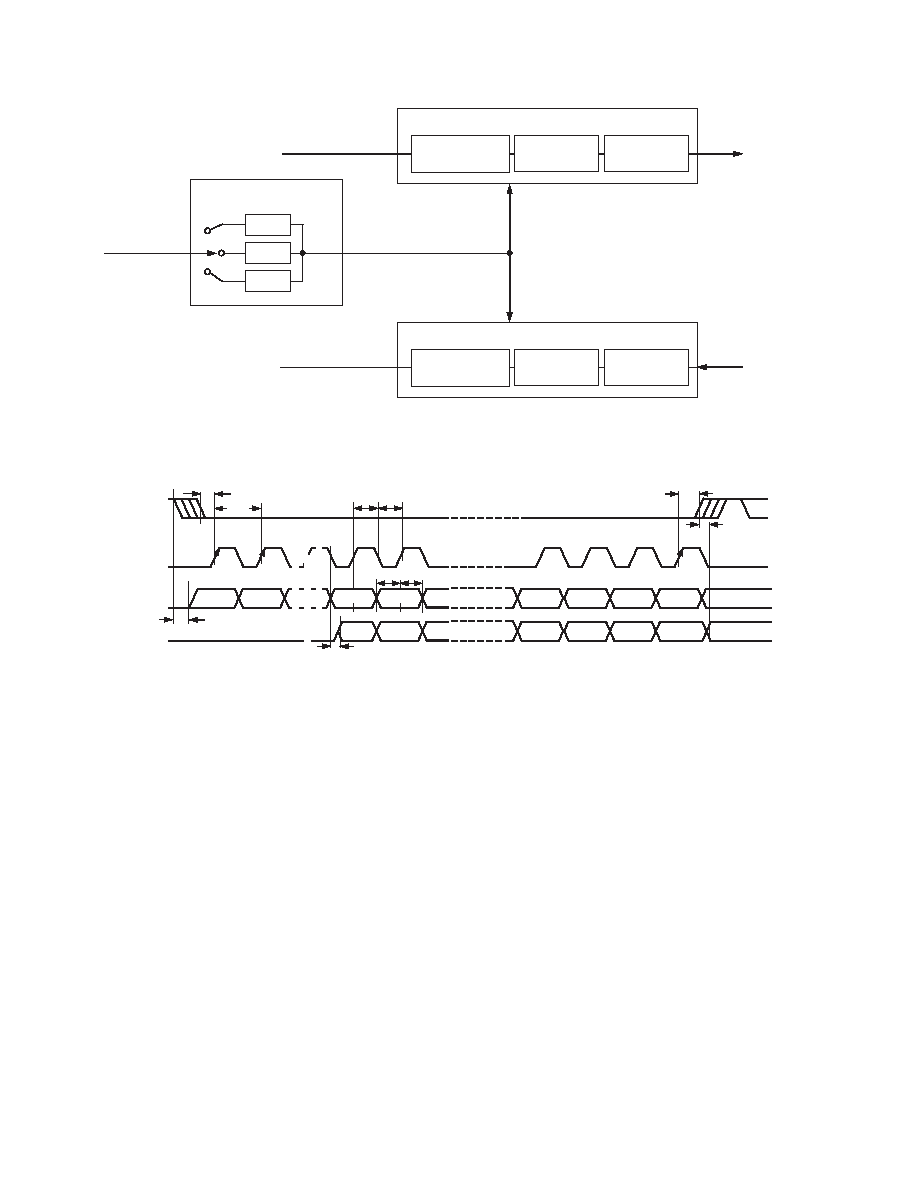
DAC ENGINE
CLOCK SCALING
1
2
2/3
MCLK
DAC INPUT
INTERPOLATION
FILTER
-
MODULATOR
DAC
48kHz/96kHz/192kHz
ADC ENGINE
ADC OUTPUT
OPTIONAL
HPF
DECIMATOR/
FILTER
48kHz/96kHz
ANALOG
OUTPUT
ANALOG
INPUT
12.288MHz
IMCLK = 24.576MHz
-
MODULATOR
Figure 2. Modulator Clocking Scheme
CLATCH
CCLK
CIN
COUT
D0
D8
D0
D15
D14
D9
D8
t
CCH tCCL
D9
t
CDS tCDH
t
CLS
t
CLH
t
COD
t
COTS
t
CCP
t
COE
Figure 3. Format of SPI Timing
相关PDF资料 |
PDF描述 |
|---|---|
| AD1835AASZ-REEL | IC CODEC 2ADC/8DAC 24BIT 52MQFP |
| ADAV803ASTZ-REEL | IC CODEC AUDIO R-DVD 3.3V 64LQFP |
| AD1939YSTZRL | IC CODEC 24BIT ADC/DAC 64-LQFP |
| AD1937WBSTZ-RL | IC CODEC 4/ADC DIFF OUT 64-LQFP |
| AD1938WBSTZ-RL | IC CODEC 24BIT 4ADC/8DAC 48LQFP |
相关代理商/技术参数 |
参数描述 |
|---|---|
| AD1838AS | 制造商:Analog Devices 功能描述:Audio Codec 2ADC / 6DAC 24-Bit 52-Pin MQFP 制造商:Rochester Electronics LLC 功能描述:- Bulk |
| AD1838AS-REEL | 制造商:Analog Devices 功能描述:Audio Codec 2ADC / 6DAC 24-Bit 52-Pin MQFP T/R 制造商:Rochester Electronics LLC 功能描述:- Tape and Reel |
| AD1839 | 制造商:AD 制造商全称:Analog Devices 功能描述:2 ADC, 6 DAC, 96 kHz, 24-Bit sigma-delta Codec |
| AD1839A | 制造商:AD 制造商全称:Analog Devices 功能描述:2 ADC, 6 DAC, 96 kHz, 24-Bit Sigma-Delta Codec |
| AD1839AAS | 制造商:Analog Devices 功能描述:Audio Codec 2ADC / 6DAC 24-Bit 52-Pin MQFP 制造商:Rochester Electronics LLC 功能描述:HIGH PERFORMANCE CODEC I.C. - Bulk 制造商:Analog Devices 功能描述:IC CODEC SMD 1839 MQFP52 |
发布紧急采购,3分钟左右您将得到回复。