参数资料
| 型号: | AD1852JRSZ |
| 厂商: | Analog Devices Inc |
| 文件页数: | 6/20页 |
| 文件大小: | 0K |
| 描述: | IC DAC STEREO 24BIT 5V 28-SSOP |
| 产品培训模块: | Data Converter Fundamentals DAC Architectures |
| 标准包装: | 47 |
| 位数: | 24 |
| 数据接口: | DSP,I²S,串行,SPI? |
| 转换器数目: | 2 |
| 电压电源: | 模拟和数字 |
| 功率耗散(最大): | 265mW |
| 工作温度: | 0°C ~ 70°C |
| 安装类型: | 表面贴装 |
| 封装/外壳: | 28-SSOP(0.209",5.30mm 宽) |
| 供应商设备封装: | 28-SSOP |
| 包装: | 管件 |
| 输出数目和类型: | 4 电压,单极 |
| 采样率(每秒): | 192k |
| 产品目录页面: | 781 (CN2011-ZH PDF) |
AD1852
Rev. A | Page 14 of 20
REGISTER ADDRESSES
The lowest two bits of the 16-bit serial control data word are
decoded as the address of the register into which the upper
14 bits are written. These bits are defined in Table 15.
Table 15. AD1852 Registers
Bit 1
Bit 0
Register
0
Volume left
1
0
Volume right
0
1
Control register
VOLUME LEFT AND VOLUME RIGHT REGISTERS
A write operation to the left or right volume registers activates
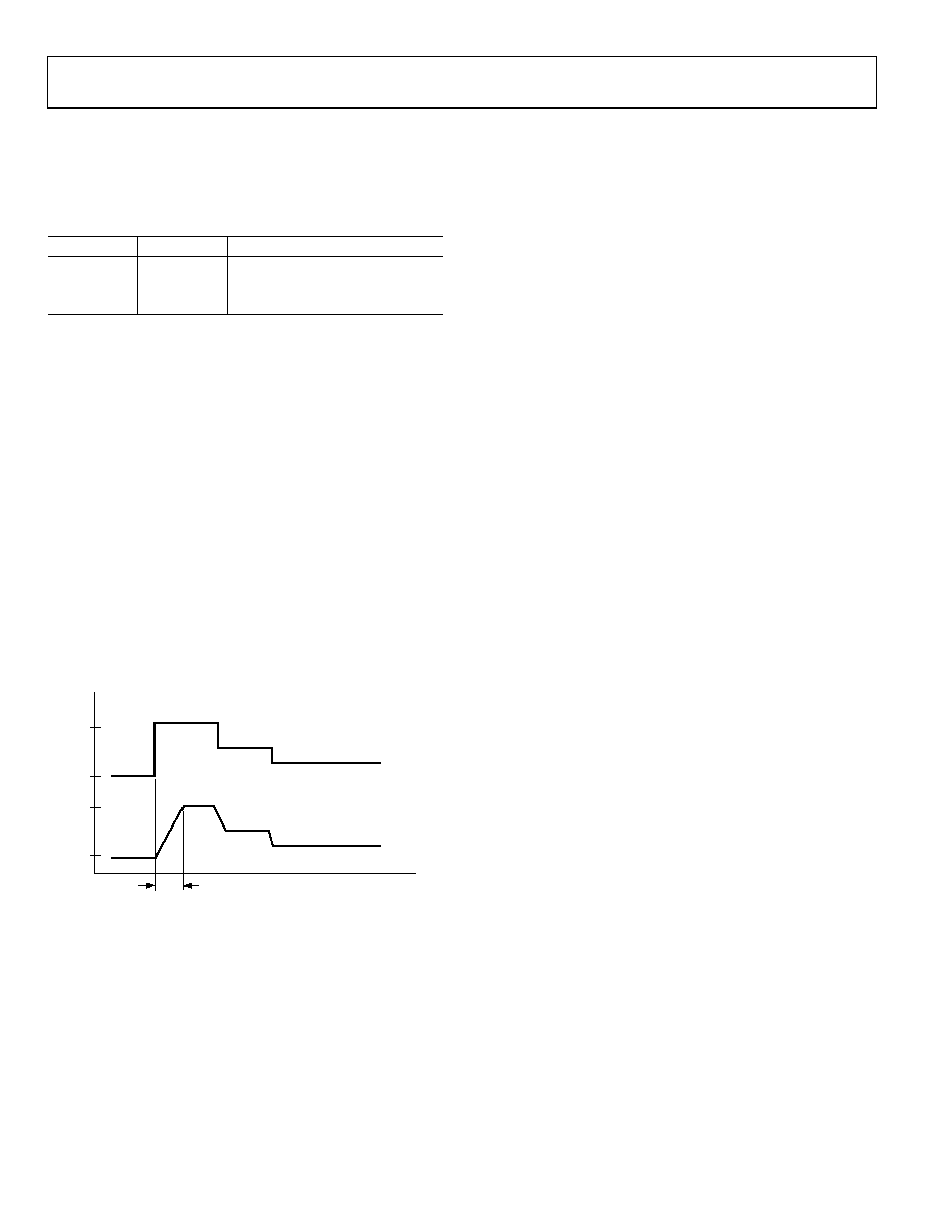
the autoramp, clickless volume control feature of the AD1852.
The upper 10 bits of the volume control word increment or
decrement by 1 at a rate equal to the input sample rate. The
bottom four bits are not fed into the autoramp circuit and thus
take effect immediately. This arrangement gives a worst-case
ramp time of about 20 ms for step changes of more than 60 dB,
which was determined by listening tests to be optimal in terms of
preventing the perception of a click sound on large volume
changes. See Figure 28 for a graphical description of how the
volume changes as a function of time.
The 14-bit volume control word is used to multiply the signal,
and therefore, the control characteristic is linear, not dB. A
constant dB/step characteristic can be obtained by using a
lookup table in the microprocessor that is writing to the SPI
port. The volume word is unsigned (that is, 0 dB is 11 1111
1111 1111).
20ms
TIME
–60
0
L
EVEL
(d
B
)
VOLUME REQUEST REGISTER
ACTUAL VOLUME REGISTER
08
457
-0
28
Figure 28. Smooth Volume Control
SPI TIMING
The SPI port is a 3-wire interface with serial data (CDATA),
serial bit clock (CCLK), and data latch (CLATCH). The data
is clocked into an internal shift register on the rising edge of
CCLK. The serial data should change on the falling edge of
CCLK and be stable on the rising edge of CCLK. The rising
edge of CLATCH is used internally to latch the parallel data
from the serial-to-parallel converter. This rising edge should be
aligned with the falling edge of the last CCLK pulse in the 16-bit
frame. The CCLK can run continuously between transactions.
Note that the serial control port timing is asynchronous to the
serial data port timing. Changes made to the attenuator level
update on the next edge of the LRCLK after the CLATCH write
pulse, as shown in Figure 27.
MUTE
The AD1852 offers two methods of muting the analog output.
By asserting the MUTE (Pin 23) signal high, both the left and
right channel are muted. As an alternative, the user can assert
the mute bit in the serial control register (Bit 6) high. The
AD1852 was designed to minimize pops and clicks when muting
and unmuting the device by automatically ramping the gain up
or down. When the device is unmuted, the volume returns to
the value set in the volume register.
相关PDF资料 |
PDF描述 |
|---|---|
| VI-B72-MY-F2 | CONVERTER MOD DC/DC 15V 50W |
| SN74AVCH4T245PWT | IC BUS TRANSCVR 4BIT 16TSSOP |
| VI-B71-MY-F2 | CONVERTER MOD DC/DC 12V 50W |
| VI-JNX-MZ-F4 | CONVERTER MOD DC/DC 5.2V 25W |
| VI-B70-MY-F2 | CONVERTER MOD DC/DC 5V 50W |
相关代理商/技术参数 |
参数描述 |
|---|---|
| AD1852JRSZ | 制造商:Analog Devices 功能描述:DAC 24BIT 192KHZ SIG DEL 28SSOP |
| AD1852JRSZRL | 功能描述:IC DAC STEREO 24BIT 28-SSOP RoHS:是 类别:集成电路 (IC) >> 数据采集 - 数模转换器 系列:- 标准包装:47 系列:- 设置时间:2µs 位数:14 数据接口:并联 转换器数目:1 电压电源:单电源 功率耗散(最大):55µW 工作温度:-40°C ~ 85°C 安装类型:表面贴装 封装/外壳:28-SSOP(0.209",5.30mm 宽) 供应商设备封装:28-SSOP 包装:管件 输出数目和类型:1 电流,单极;1 电流,双极 采样率(每秒):* |
| AD1853 | 制造商:AD 制造商全称:Analog Devices 功能描述:Stereo, 24-Bit, 192 kHz, Multibit DAC |
| AD1853JRS | 制造商:Analog Devices 功能描述:DAC 2-CH Delta-Sigma 24-bit 28-Pin SSOP 制造商:Rochester Electronics LLC 功能描述:STEREO, 192KHZ MULTIBIT SIGMA DELTA DAC - Bulk 制造商:Analog Devices 功能描述:IC STEREO 24-BIT DAC |
发布紧急采购,3分钟左右您将得到回复。