- 您现在的位置:买卖IC网 > PDF目录2062 > AD1895AYRSZRL (Analog Devices Inc)IC SAMP-RATEHP/CONV 24BIT 28SSOP PDF资料下载
参数资料
| 型号: | AD1895AYRSZRL |
| 厂商: | Analog Devices Inc |
| 文件页数: | 11/24页 |
| 文件大小: | 0K |
| 描述: | IC SAMP-RATEHP/CONV 24BIT 28SSOP |
| 标准包装: | 1,500 |
| 类型: | 采样率转换器 |
| 应用: | 车载音频,接收器,机顶盒 |
| 安装类型: | 表面贴装 |
| 封装/外壳: | 28-SSOP(0.209",5.30mm 宽) |
| 供应商设备封装: | 28-SSOP |
| 包装: | 带卷 (TR) |
REV. B
AD1895
–19–
OPERATING FEATURES
RESET and Power-Down
When
RESET is asserted low, the AD1895 will turn off the
master clock input to the AD1895, MCLK_IN, initialize all of its
internal registers to their default values, and three-state all of the
I/O pins. While
RESET is active low, the AD1895 is consuming
minimum power. For the lowest possible power consumption
while
RESET is active low, all of the input pins to the AD1895
should be static.
When
RESET is deasserted, the AD1895 begins its initialization
routine where all locations in the FIFO are initialized to zero,
MUTE_OUT is asserted high, and any I/O pins configured as
outputs are enabled. The mute control counter, which controls
the soft mute attenuation of the input samples, is initialized to
maximum attenuation, –127 dB (see Mute Control section).
When asserting
RESET and deasserting RESET, the RESET
should be held low for a minimum of five MCLK_IN cycles.
During power-up, the
RESET should be held low until the power
supplies have stabilized. It is recommended that the AD1895 be
reset when changing modes.
Power Supply and Voltage Reference
The AD1895 is designed for 3 V operation with 5 V input toler-
ance on the input pins. VDD_CORE is the 3 V supply that is used
to power the core logic of the AD1895 and to drive the output
pins. VDD_IO is used to set the input voltage tolerance of the
input pins. In order for the input pins to be 5 V input tolerant,
VDD_IO must be connected to a 5 V supply. If the input pins do
not have to be 5 V input tolerant, then VDD_IO can be connected
to VDD_CORE. VDD_IO should never be less than VDD_CORE.
VDD_CORE and VDD_IO should be bypassed with 100 nF
ceramic chip capacitors as close to the pins as possible to minimize
power supply and ground bounce caused by inductance in the
traces. A bulk aluminium electrolytic capacitor of 47
F should
also be provided on the same PC board as the AD1895.
Digital Filter Group Delay
The filter group delay is given by the equation:
GD
ff
for f
f
GD
ff
f
for f
f
SIN
S
OUT
S
IN
SIN
S
OUT
S
OUT
S
IN
=+
>
=+
×
<
16
32
16
32
__
_
__
seconds
Mute Control
When the MUTE_IN pin is asserted high, the MUTE_IN control
will perform a soft mute by linearly decreasing the input data to the
AD1895 FIFO to almost zero, –127 dB attenuation. When
MUTE_IN is deasserted low, the MUTE_IN control will linearly
decrease the attenuation of the input data to 0 dB. A 12-bit counter,
clocked by LRCLK_I, is used to control the mute attenuation.
Therefore, the time it will take from the assertion of MUTE_IN
to –127 dB full mute attenuation is 4096/LRCLK_I seconds.
Likewise, the time it will take to reach 0 dB mute attenuation from
the deassertion of MUTE_IN is 4096/LRCLK_I seconds.
Upon RESET, or a change in the sample rate between LRCLK_I
and LRCLK_O, the MUTE_OUT pin will be asserted high. The
MUTE_OUT pin will remain asserted high until the digital servo
loop’s internal Fast Settling Mode has completed. When the digital
servo loop has switched to Slow Settling Mode, the MUTE_OUT
pin will deassert. While MUTE_OUT is asserted, the MUTE_IN
pin should be asserted as well to prevent any major distortion in
the audio output samples.
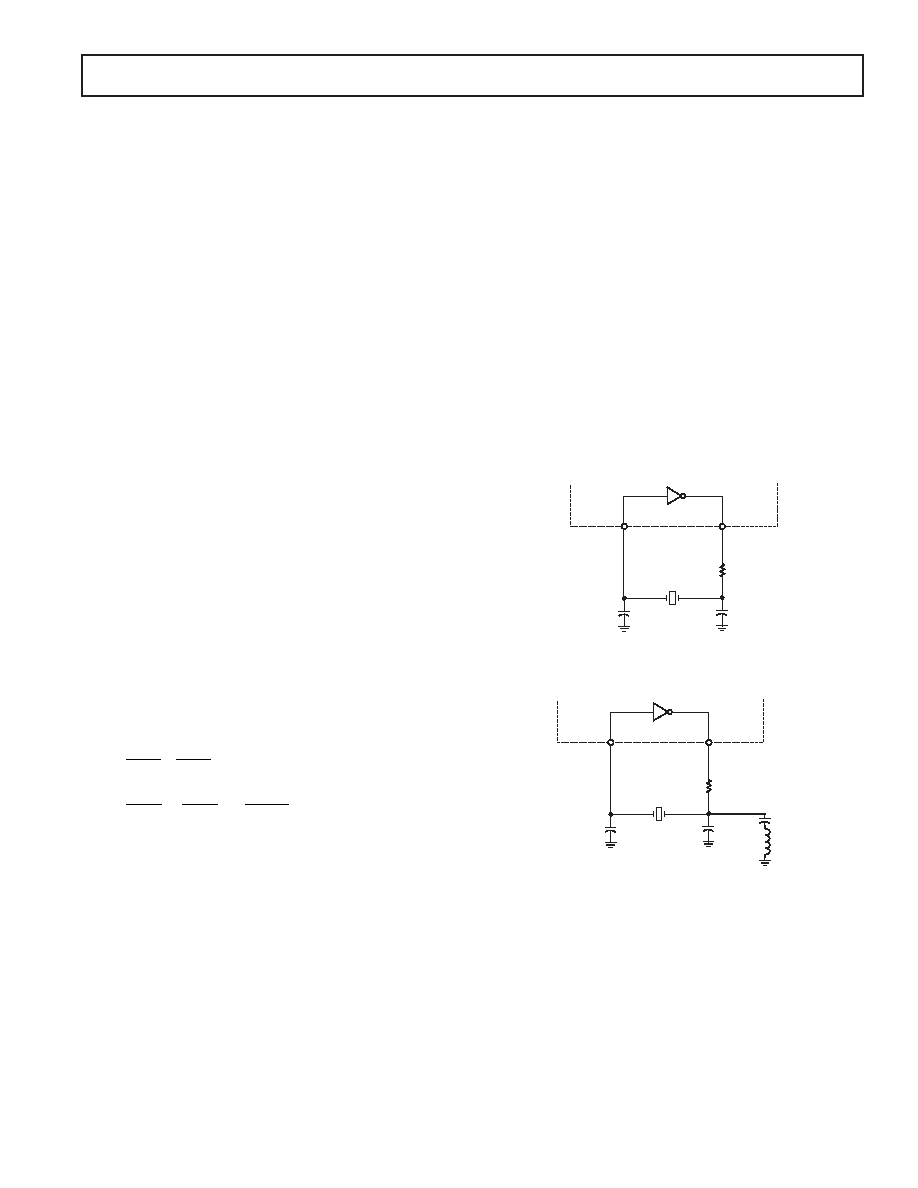
Master Clock
A digital clock connected to the MCLK_IN pin or a fundamental
or third overtone crystal connected between MCLK_IN and
MCLK_OUT can be used to generate the master clock, MCLK_IN.
The MCLK_IN pin can be 5 V input tolerant just like any of
the other AD1895 input pins. A fundamental mode crystal can
be inserted between MCLK_IN and MCLK_OUT for master
clock frequency generation up to 27 MHz. For master clock
frequency generation with a crystal beyond 27 MHz, it is recom-
mended that the user use a third overtone crystal and add an
LC filter at the output of MCLK_OUT to filter out the fundamental,
do not notch filter the fundamental. Please refer to your quartz
crystal supplier for values for external capacitors and inductor
components.
AD1895
MCLK_IN
MCLK_OUT
C1
C2
R
Figure 9a. Fundamental Mode Circuit Configuration
AD1895
MCLK_IN
MCLK_OUT
C1
C2
R
1nF
L1
Figure 9b. Third Overtone Circuit Configuration
There are, of course, maximum and minimum operating fre-
quencies for the AD1895 master clock. The maximum master
clock frequency at which the AD1895 is guaranteed to operate is
30 MHz. 30 MHz is more than sufficient to sample rate convert
sampling frequencies of 192 kHz + 12%. The minimum required
frequency for the master clock generation for the AD1895 depends
upon the input and output sample rates. The master clock has
to be at least 138 times greater than the maximum input or
output sample rate.
相关PDF资料 |
PDF描述 |
|---|---|
| AD1896AYRSZRL | IC SAMP-RATEHP/CONV 24BIT 28SSOP |
| AD1940YSTZ | IC DSP AUDIO 16CH/28BIT 48-LQFP |
| AD246JY | IC CLK BUFF DVR 1:1 25KHZ 13-SIP |
| AD532SD | IC MULTIPLIER +/-10V 14-CDIP |
| AD534TD | IC PREC MULTIPLIER 14-CDIP |
相关代理商/技术参数 |
参数描述 |
|---|---|
| AD1895YRS | 制造商:Rochester Electronics LLC 功能描述:192KHZ 8:1 STEREO ASYNC S - Bulk |
| AD1895YRSRL | 制造商:Rochester Electronics LLC 功能描述:192KHZ 8:1 STEREO ASYNC S - Bulk |
| AD1896 | 制造商:AD 制造商全称:Analog Devices 功能描述:192 kHz Stereo Asynchronous Sample Rate Converter |
| AD1896AYRS | 制造商:Analog Devices 功能描述:Sample Rate Converter 28-Pin SSOP 制造商:Rochester Electronics LLC 功能描述:192KHZ 8:1 STEREO ASYNC SAMPLE RATE CONV - Bulk 制造商:Analog Devices 功能描述:IC STEREO ASR CONVERTER |
| AD1896AYRSRL | 制造商:Analog Devices 功能描述:Sample Rate Converter 28-Pin SSOP T/R |
发布紧急采购,3分钟左右您将得到回复。