- 您现在的位置:买卖IC网 > PDF目录1888 > AD1934WBSTZ-RL (Analog Devices Inc)IC DAC 8CH W/ON-CHIP PLL 48LQFP PDF资料下载
参数资料
| 型号: | AD1934WBSTZ-RL |
| 厂商: | Analog Devices Inc |
| 文件页数: | 6/28页 |
| 文件大小: | 0K |
| 描述: | IC DAC 8CH W/ON-CHIP PLL 48LQFP |
| 标准包装: | 2,000 |
| 位数: | 24 |
| 数据接口: | 串行,SPI? |
| 转换器数目: | 8 |
| 电压电源: | 模拟和数字 |
| 工作温度: | -40°C ~ 105°C |
| 安装类型: | 表面贴装 |
| 封装/外壳: | 48-LQFP |
| 供应商设备封装: | 48-LQFP(7x7) |
| 包装: | 带卷 (TR) |
| 输出数目和类型: | 8 电压,单极 |
| 采样率(每秒): | * |
第1页第2页第3页第4页第5页当前第6页第7页第8页第9页第10页第11页第12页第13页第14页第15页第16页第17页第18页第19页第20页第21页第22页第23页第24页第25页第26页第27页第28页
AD1934
Data Sheet
Rev. D | Page 14 of 28
POWER SUPPLY AND VOLTAGE REFERENCE
The AD1934 is designed for 3.3 V supplies. Separate power
supply pins are provided for the analog and digital sections.
These pins should be bypassed with 100 nF ceramic chip
capacitors, as close to the pins as possible, to minimize noise
pickup. A bulk aluminum electrolytic capacitor of at least 22 μF
should also be provided on the same PC board as the DAC. For
critical applications, improved performance is obtained with
separate supplies for the analog and digital sections. If this is
not possible, it is recommended that the analog and digital
supplies be isolated by means of a ferrite bead in series with
each supply. It is important that the analog supply be as
clean as possible.
All digital inputs are compatible with TTL and CMOS levels.
All outputs are driven from the 3.3 V DVDD supply and are
compatible with TTL and 3.3 V CMOS levels.
The DAC internal voltage reference (VREF) is brought out on
FILTR and should be bypassed as close as possible to the chip,
with a parallel combination of 10 μF and 100 nF. Any external
current drawn should be limited to less than 50 μA.
The internal reference can be disabled in PLL and Clock
Control 1 Register and FILTR can be driven from an external
source. This can be used to scale the DAC output to the clipping
level of a power amplifier based on its power supply voltage.
The CM pin is the internal common-mode reference. It should
be bypassed as close as possible to the chip, with a parallel
combination of 47 μF and 100 nF. This voltage can be used to
bias external op amps to the common-mode voltage of the input
and output signal pins. The output current should be limited to
less than 0.5 mA source and 2 mA sink.
SERIAL DATA PORTS—DATA FORMAT
The eight DAC channels use a common serial bit clock (DBCLK)
and a common left-right framing clock (DLRCLK) in the serial
data port. The clock signals are all synchronous with the sample
rate. The normal stereo serial modes are shown in Figure 15.
The DAC serial data modes default to I2S. The ports can also be
programmed for left-justified, right-justified, and TDM modes.
The word width is 24 bits by default and can be programmed
for 16 or 20 bits. The DAC serial formats are programmable
according to DAC Control 0 Register. The polarity of the
DBCLK and DLRCLK is programmable according to DAC
Control 1 Register. The auxiliary TDM port is also provided for
applications requiring more than eight DAC channels. In this
mode, the AUXTDMLRCLK and AUXTDMBCLK pins are
configured as TDM port clocks. In regular TDM mode, the
DLRCLK and DBCLK pins are used as the TDM port clocks.
The auxiliary TDM serial port’s format and its serial clock
polarity is programmable according to the Auxiliary TDM Port
Control 0 Register and Control 1 Register. Both DAC and
auxiliary TDM serial ports are programmable to become the
bus masters according to DAC Control 1 Register and auxiliary
TDM Control 1 Register. By default, both auxiliary TDM and
DAC serial ports are in the slave mode.
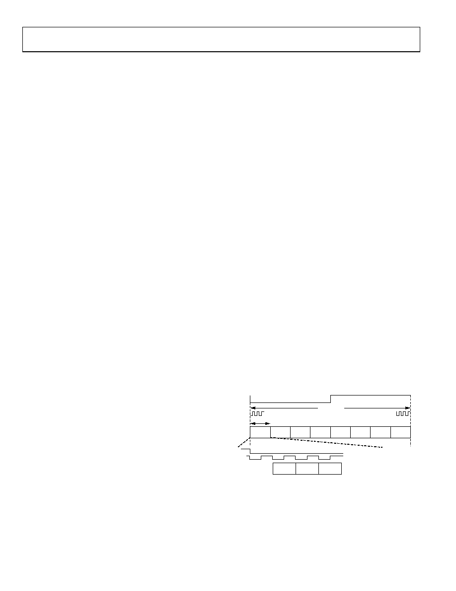
TIME-DIVISION MULTIPLEXED (TDM) MODES
The AD1934 serial ports also have several different TDM serial
data modes. The most commonly used configuration is shown
in Figure 10. In Figure 10, the eight on-chip DAC data slots are
packed into one TDM stream. In this mode, DBCLK is 256 fS.
The I/O pins of the serial ports are defined according to the
serial mode selected. For a detailed description of the function
of each pin in TDM and AUX Modes, see Table 12.
The AD1934 allows systems with more than eight DAC channels
to be easily configured by the use of an auxiliary serial data port.
The DAC TDM-AUX mode is shown in Figure 11. In this mode,
the AUX channels are the last four slots of the 16-channel TDM
data stream. These slots are extracted and output to the AUX
serial port. One major difference between the TDM mode and
an auxiliary TDM mode is the assignment of the TDM port
pins, as shown in Table 12. In auxiliary TDM mode, DBCLK
and DLRCLK are assigned as the auxiliary port clocks, and
AUXTDMBCLK and AUXTDMLRCLK are assigned as the
TDM port clocks. In regular TDM or 16-channel, daisy-chain
TDM mode, the DLRCLK and DBCLK pins are set as the TDM
port clocks. It should be noted that due to the high
AUXTDMBCLK frequency, 16-channel auxiliary TDM mode is
available only in the 48 kHz/44.1 kHz/32 kHz sample rate.
SLOT 1
LEFT 1
SLOT 2
RIGHT 1
SLOT 3
LEFT 2
SLOT 4
RIGHT 2
MSB
MSB–1
MSB–2
DATA
BCLK
LRCLK
SLOT 5
LEFT 3
SLOT 6
RIGHT 3
SLOT 7
LEFT 4
SLOT 8
RIGHT 4
LRCLK
BCLK
DATA
256 BCLKs
32 BCLK
06106-
017
Figure 10. DAC TDM (8-Channel I2S Mode)
相关PDF资料 |
PDF描述 |
|---|---|
| AD1937WBSTZ | IC CODEC 4/ADC DIFF OUT 64-LQFP |
| AD1938WBSTZ | IC CODEC 24BIT 4ADC/8DAC 48LQFP |
| AD1939WBSTZ-RL | AUDIO CODEC W/ON CHIP 4ADC 8DAC |
| AD1953YSTZ | IC DSP DAC AUDIO3CH/26BIT 48LQFP |
| AD1954YSTZRL | IC DAC AUDIO 3CHAN 26BIT 48LQFP |
相关代理商/技术参数 |
参数描述 |
|---|---|
| AD1934YSTZ | 功能描述:IC DAC 8CH W/ON-CHIP PLL 48LQFP RoHS:是 类别:集成电路 (IC) >> 数据采集 - 数模转换器 系列:- 产品培训模块:Lead (SnPb) Finish for COTS Obsolescence Mitigation Program 标准包装:50 系列:- 设置时间:4µs 位数:12 数据接口:串行 转换器数目:2 电压电源:单电源 功率耗散(最大):- 工作温度:-40°C ~ 85°C 安装类型:表面贴装 封装/外壳:8-TSSOP,8-MSOP(0.118",3.00mm 宽) 供应商设备封装:8-uMAX 包装:管件 输出数目和类型:2 电压,单极 采样率(每秒):* 产品目录页面:1398 (CN2011-ZH PDF) |
| AD1934YSTZ-RL | 制造商:Rochester Electronics LLC 功能描述: 制造商:Analog Devices 功能描述: |
| AD1935 | 制造商:AD 制造商全称:Analog Devices 功能描述:4 ADC/8 DAC with PLL, 192 kHz, 24 Bit CODEC |
| AD1935XSTZ | 制造商:AD 制造商全称:Analog Devices 功能描述:4 ADC/8 DAC with PLL, 192 kHz, 24 Bit CODEC |
| AD1935XSTZRL | 制造商:AD 制造商全称:Analog Devices 功能描述:4 ADC/8 DAC with PLL, 192 kHz, 24 Bit CODEC |
发布紧急采购,3分钟左右您将得到回复。