- 您现在的位置:买卖IC网 > PDF目录8647 > AD5045BRUZ-REEL7 (Analog Devices Inc)IC DAC DUAL 14BIT SPI 14TSSOP PDF资料下载
参数资料
| 型号: | AD5045BRUZ-REEL7 |
| 厂商: | Analog Devices Inc |
| 文件页数: | 14/28页 |
| 文件大小: | 0K |
| 描述: | IC DAC DUAL 14BIT SPI 14TSSOP |
| 产品培训模块: | Data Converter Fundamentals DAC Architectures |
| 标准包装: | 1,000 |
| 系列: | nanoDAC™ |
| 设置时间: | 5.8µs |
| 位数: | 14 |
| 数据接口: | 串行,SPI? |
| 转换器数目: | 2 |
| 电压电源: | 单电源 |
| 功率耗散(最大): | 13.5mW |
| 工作温度: | -40°C ~ 125°C |
| 安装类型: | 表面贴装 |
| 封装/外壳: | 14-TSSOP(0.173",4.40mm 宽) |
| 供应商设备封装: | 14-TSSOP |
| 包装: | 带卷 (TR) |
| 输出数目和类型: | 2 电压,单极;2 电压,双极 |
| 采样率(每秒): | * |
第1页第2页第3页第4页第5页第6页第7页第8页第9页第10页第11页第12页第13页当前第14页第15页第16页第17页第18页第19页第20页第21页第22页第23页第24页第25页第26页第27页第28页
AD5025/AD5045/AD5065
Rev. 0 | Page 21 of 28
CLEAR CODE REGISTER
The AD5025/AD5045/AD5065 have a hardware CLR pin that
is an asynchronous clear input. The CLR input is falling edge sensi-
tive. Bringing the CLR line low clears the contents of the input
register and the DAC registers to the data contained in the user-
configurable CLR register, and sets the analog outputs accordingly
(see Table 13). This function can be used in system calibration
to load zero scale, midscale, or full scale to all channels together.
These clear code values are user-programmable by setting two
bits, Bit DB1 and Bit DB0, in the input register (see Table 13).
The default setting clears the outputs to 0 V. Command 0101 is
reserved for loading the clear code register (see Table 8).
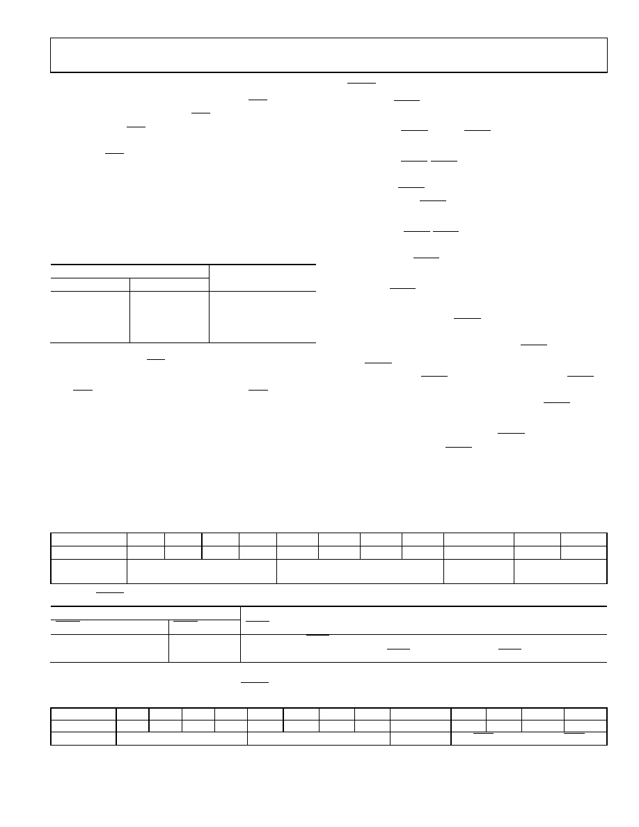
Table 13. Clear Code Register
Clear Code Register
DB1 (CR1)
DB0 (CR0)
Clears to Code
0
0x0000
0
1
0x8000
1
0
0xFFFF
1
No operation
The part exits clear code mode on the 32nd falling edge of the
next write to the part. If CLR is activated during a write sequence,
the write is aborted.
The CLR pulse activation time, the falling edge of CLR to when
the output starts to change, is typically 10.6 μs (see Figure 31).
See Table 14 for contents of the input register during the
loading clear code register operation.
LDAC FUNCTION
Hardware LDAC Pin
The outputs of all DACs can be updated simultaneously using
the hardware LDAC pin. The LDAC pin can be used in
synchronous or asynchronous mode, as shown in Figure 3.
Synchronous LDAC: LDAC is held low. After new data is read,
the DAC registers are updated on the falling edge of the 32nd
SCLK pulse. LDAC can be permanently low or pulsed in
standalone mode. LDAC cannot be tied permanently low in
daisy-chain mode.
Asynchronous LDAC: LDAC is held high and pulsed. The outputs
are not updated at the same time that the input registers are
written to. When LDAC goes low, the DAC registers are updated
with the contents of the input register.
Software LDAC Function
Alternatively, the outputs of all DACs can be updated simulta-
neously using the software LDAC function by writing to Input
Register n (see Table 7) and updating all DAC registers.
Command 0010 is reserved for this software LDAC function.
The LDAC register gives the user extra flexibility and control
over the hardware LDAC pin (see Table 16). Setting the LDAC
bit register (DB0 to DB3) to 0 for a DAC channel means that
this channel update is controlled by the hardware LDAC pin.
If DB0 or DB3 is set to 1, this channel updates synchronously.
The part effectively sees the hardware LDAC pin as being tied
low (see Table 15 for the LDAC register mode of operation).
This flexibility is useful in applications where the user wants to
simultaneously update select channels while the rest of the
channels are synchronously updating.
Table 14. 32-Bit Input Register Contents for Clear Code Function
MSB
LSB
DB31 to DB28
DB27
DB26
DB25
DB24
DB23
DB22
DB21
DB20
DB2 to DB19
DB1
DB0
X
0
1
0
1
X
1/0
Don’t cares
Command bits (C3 to C0)
Address bits (A3 to A0)
Don’t cares
Clear code register
(CR1 to CR0)
Table 15. LDAC Overwrite Definitions
Load DAC Register
LDAC Bits (DB3 and DB0)
LDAC Pin
LDAC Operation
0
1, 0
Determined by LDAC pin.
1
X1
DAC channels update, overrides the LDAC pin. DAC channels see LDAC as 0.
1 X = don’t care.
Table 16. 32-Bit Input Register Contents for LDAC Overwrite Function
MSB
LSB
DB31 to DB28
DB27
DB26
DB25
DB24
DB23
DB22
DB21
DB20
DB4 to DB19
DB3
DB2
DB1
DB0
X
0
1
0
X
DAC B
X
DAC A
Don’t cares
Command bits (C3 to C0)
Address bits (A3 to A0)—don’t cares
Don’t cares
Set LDAC bits to 1 to override LDAC pin
相关PDF资料 |
PDF描述 |
|---|---|
| LTC2614CGN#TRPBF | IC DAC 14BIT QUAD R-R OUT 16SSOP |
| VE-J60-MZ-B1 | CONVERTER MOD DC/DC 5V 25W |
| VE-J5D-MZ-B1 | CONVERTER MOD DC/DC 85V 25W |
| VI-26P-MW-B1 | CONVERTER MOD DC/DC 13.8V 100W |
| VI-J5D-MZ-B1 | CONVERTER MOD DC/DC 85V 25W |
相关代理商/技术参数 |
参数描述 |
|---|---|
| AD504KH | 制造商:Rochester Electronics LLC 功能描述:- Bulk |
| AD504LH | 制造商:Rochester Electronics LLC 功能描述:- Bulk |
| AD504MH | 制造商:Rochester Electronics LLC 功能描述:- Bulk |
| AD504SH | 制造商:Rochester Electronics LLC 功能描述:- Bulk |
| AD505-00E | 功能描述:SENSOR MAG SW 40G STANDRD 8-MSOP 制造商:nve corp/sensor products 系列:AD 包装:管件 零件状态:有效 功能:全极开关 技术:霍尔效应 极化:任意一种 感应范围:±5mT 跳闸,±2.5mT 释放 测试条件:-40°C ~ 125°C 电压 - 电源:4.5 V ~ 30 V 电流 - 电源(最大值):4.5mA 电流 - 输出(最大值):20mA 输出类型:开路集电极 特性:- 工作温度:-40°C ~ 125°C(TA) 封装/外壳:8-TSSOP,8-MSOP(0.118",3.00mm 宽) 供应商器件封装:8-MSOP 标准包装:1,000 |
发布紧急采购,3分钟左右您将得到回复。