- 您现在的位置:买卖IC网 > PDF目录8596 > AD5064ARUZ-1REEL7 (Analog Devices Inc)IC DAC 16BIT 4CH BUF OUT 14TSSOP PDF资料下载
参数资料
| 型号: | AD5064ARUZ-1REEL7 |
| 厂商: | Analog Devices Inc |
| 文件页数: | 11/28页 |
| 文件大小: | 0K |
| 描述: | IC DAC 16BIT 4CH BUF OUT 14TSSOP |
| 产品培训模块: | Data Converter Fundamentals DAC Architectures |
| 标准包装: | 1,000 |
| 系列: | nanoDAC™ |
| 设置时间: | 5.8µs |
| 位数: | 16 |
| 数据接口: | 串行 |
| 转换器数目: | 4 |
| 电压电源: | 单电源 |
| 功率耗散(最大): | 30mW |
| 工作温度: | -40°C ~ 125°C |
| 安装类型: | 表面贴装 |
| 封装/外壳: | 14-TSSOP(0.173",4.40mm 宽) |
| 供应商设备封装: | 14-TSSOP |
| 包装: | 带卷 (TR) |
| 输出数目和类型: | 4 电压,双极 |
| 采样率(每秒): | 125k |
第1页第2页第3页第4页第5页第6页第7页第8页第9页第10页当前第11页第12页第13页第14页第15页第16页第17页第18页第19页第20页第21页第22页第23页第24页第25页第26页第27页第28页
Data Sheet
AD5024/AD5044/AD5064
Rev. F | Page 19 of 28
THEORY OF OPERATION
DIGITAL-TO-ANALOG CONVERTER
The AD5024/AD5044/AD5064/AD5064-1 are single 12-/14-/
16-bit, serial input, voltage output DACs with an individual
reference pin. The AD5064-1 model (see the Ordering Guide)
is a 16-bit, serial input, voltage output DAC that is identical to
other AD5064 models but with a single reference pin for all
DACs. The parts operate from supply voltages of 4.5 V to 5.5 V.
Data is written to the AD5024/AD5044/AD5064/AD5064-1 in a
32-bit word format via a 3-wire serial interface. The AD5024/
AD5044/AD5064/AD5064-1 incorporate a power-on reset circuit
that ensures that the DAC output powers up to a known output
state. The devices also have a software power-down mode that
reduces the typical current consumption to typically 400 nA.
Because the input coding to the DAC is straight binary, the ideal
output voltage when using an external reference is given by
×
=
N
REFIN
OUT
D
V
2
where:
D is the decimal equivalent of the binary code that is loaded to
the DAC register (0 to 65,535 for the 16-bit AD5064).
N is the DAC resolution.
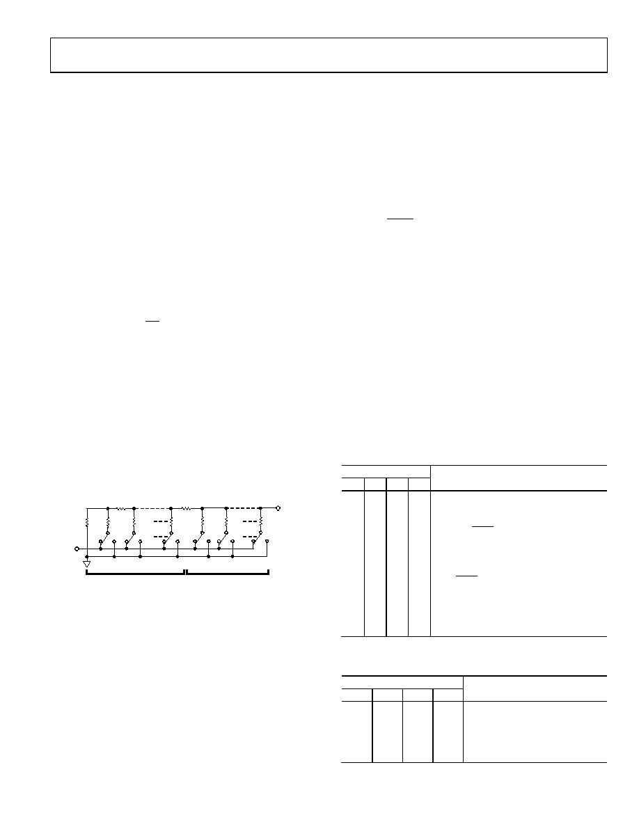
DAC ARCHITECTURE
The DAC architecture of the AD5064 consists of two matched
DAC sections. A simplified circuit diagram is shown in Figure 46.
The four MSBs of the 16-bit data word are decoded to drive
15 switches, E1 to E15. Each of these switches connects one of
15 matched resistors to either GND or the VREF buffer output.
The remaining 12 bits of the data-word drive the S0 to S11
switches of a 12-bit voltage mode R-2R ladder network.
2R
S0
VREF
2R
S1
2R
S11
2R
E1
2R
E2
2R
E15
2R
VOUT
12-BIT R-2R LADDER
FOUR MSBs DECODED INTO
15 EQUAL SEGMENTS
06803-
006
Figure 46. DAC Ladder Structure
REFERENCE BUFFER
The AD5024/AD5044/AD5064/AD5064-1 operate with an exter-
nal reference. For most models, each DAC has a dedicated voltage
reference pin. The AD5064-1 model has a single voltage reference
pin for all DACs. The reference input pin has an input range of
2.2 V to VDD. This input voltage is then buffered internally to
provide a reference for the DAC core.
OUTPUT AMPLIFIER
The output buffer amplifier can generate rail-to-rail voltages
on its output, which gives an output range of 0 V to VDD. The
amplifier is capable of driving a load of 5 k in parallel with
200 pF to GND. The slew rate is 1.5 V/s with a to scale
settling time of 5.8 s.
SERIAL INTERFACE
The AD5024/AD5044/AD5064/AD5064-1 have a 3-wire serial
interface (SYNC, SCLK, and DIN) that is compatible with SPI,
QSPI, and MICROWIRE interface standards as well as most
DSPs. See Figure 4 for a timing diagram of a typical write
sequence. The AD5064-1 model contains an SDO pin to allow
the user to daisy-chain multiple devices together (see the Daisy-
Chaining section).
SHIFT REGISTER
The AD5024/AD5044/AD5064/AD5064-1 shift register is 32 bits
wide. The first four bits are don’t cares. The next four bits are the
command bits, C3 to C0 (see Table 8), followed by the 4-bit
DAC address bits, A3 to A0 (see Table 9), and finally the bit
data-word. The data-word comprises 12-bit, 14-bit, or 16-bit input
code, followed by eight, six, or four don’t care bits for the AD5024,
AD5044, and AD5064/AD5064-1, respectively (see Figure 47,
Figure 48, and Figure 49). These data bits are transferred to the
DAC register on the 32nd falling edge of SCLK. Commands can be
executed on individually selected DAC channels or on all DACs.
Table 8. Command Definitions
Command
C3
C2
C1
C0
Description
0
Write to Input Register n
0
1
Update DAC Register n
0
1
0
Write to Input Register n, update all
(software LDAC)
0
1
Write to and update DAC Channel n
0
1
0
Power down/power up DAC
0
1
0
1
Load clear code register
0
1
0
Load LDAC register
0
1
Reset (power-on reset)
1
0
Set up DCEN register1 (daisy-chain enable)
1
0
1
Reserved
1
Reserved
1
Available in the AD5064-1 14-lead TSSOP package only.
Table 9. Address Commands
Address (n)
Selected DAC Channel
A3
A2
A1
A0
0
DAC A
0
1
DAC B
0
1
0
DAC C
0
1
DAC D
1
All DACs
相关PDF资料 |
PDF描述 |
|---|---|
| AD8582AR-REEL | IC DAC DUAL 12BIT 5V 24SOIC |
| AD7225LRZ | IC DAC 8BIT QUAD W/AMP 24SOIC |
| VI-B3Y-MY-B1 | CONVERTER MOD DC/DC 3.3V 33W |
| AD7541AKN | IC DAC 12BIT MULTIPLYING 18-DIP |
| VI-B3Z-MY-B1 | CONVERTER MOD DC/DC 2V 20W |
相关代理商/技术参数 |
参数描述 |
|---|---|
| AD5064BRUZ | 功能描述:IC DAC 16BIT 4CH BUF OUT 16TSSOP RoHS:是 类别:集成电路 (IC) >> 数据采集 - 数模转换器 系列:nanoDAC™ 产品培训模块:Lead (SnPb) Finish for COTS Obsolescence Mitigation Program 标准包装:50 系列:- 设置时间:4µs 位数:12 数据接口:串行 转换器数目:2 电压电源:单电源 功率耗散(最大):- 工作温度:-40°C ~ 85°C 安装类型:表面贴装 封装/外壳:8-TSSOP,8-MSOP(0.118",3.00mm 宽) 供应商设备封装:8-uMAX 包装:管件 输出数目和类型:2 电压,单极 采样率(每秒):* 产品目录页面:1398 (CN2011-ZH PDF) |
| AD5064BRUZ-1 | 功能描述:IC DAC 16BIT 4CH BUF OUT 14TSSOP RoHS:是 类别:集成电路 (IC) >> 数据采集 - 数模转换器 系列:nanoDAC™ 产品培训模块:Lead (SnPb) Finish for COTS Obsolescence Mitigation Program 标准包装:50 系列:- 设置时间:4µs 位数:12 数据接口:串行 转换器数目:2 电压电源:单电源 功率耗散(最大):- 工作温度:-40°C ~ 85°C 安装类型:表面贴装 封装/外壳:8-TSSOP,8-MSOP(0.118",3.00mm 宽) 供应商设备封装:8-uMAX 包装:管件 输出数目和类型:2 电压,单极 采样率(每秒):* 产品目录页面:1398 (CN2011-ZH PDF) |
| AD5064BRUZ-1REEL7 | 功能描述:IC DAC 16BIT 4CH BUF OUT 14TSSOP RoHS:是 类别:集成电路 (IC) >> 数据采集 - 数模转换器 系列:nanoDAC™ 产品培训模块:Data Converter Fundamentals DAC Architectures 标准包装:750 系列:- 设置时间:7µs 位数:16 数据接口:并联 转换器数目:1 电压电源:双 ± 功率耗散(最大):100mW 工作温度:0°C ~ 70°C 安装类型:表面贴装 封装/外壳:28-LCC(J 形引线) 供应商设备封装:28-PLCC(11.51x11.51) 包装:带卷 (TR) 输出数目和类型:1 电压,单极;1 电压,双极 采样率(每秒):143k |
| AD5064BRUZ-REEL7 | 功能描述:IC DAC 16BIT 4CH BUF OUT 16TSSOP RoHS:是 类别:集成电路 (IC) >> 数据采集 - 数模转换器 系列:nanoDAC™ 产品培训模块:Data Converter Fundamentals DAC Architectures 标准包装:750 系列:- 设置时间:7µs 位数:16 数据接口:并联 转换器数目:1 电压电源:双 ± 功率耗散(最大):100mW 工作温度:0°C ~ 70°C 安装类型:表面贴装 封装/外壳:28-LCC(J 形引线) 供应商设备封装:28-PLCC(11.51x11.51) 包装:带卷 (TR) 输出数目和类型:1 电压,单极;1 电压,双极 采样率(每秒):143k |
| AD5065 | 制造商:AD 制造商全称:Analog Devices 功能描述:Fully Accurate, 12-/14-/16-Bit, Dual, VOUT nanoDAC SPI Interface, 4.5 V to 5.5 V in a TSSOP |
发布紧急采购,3分钟左右您将得到回复。