- 您现在的位置:买卖IC网 > PDF目录8596 > AD5064ARUZ-1REEL7 (Analog Devices Inc)IC DAC 16BIT 4CH BUF OUT 14TSSOP PDF资料下载
参数资料
| 型号: | AD5064ARUZ-1REEL7 |
| 厂商: | Analog Devices Inc |
| 文件页数: | 15/28页 |
| 文件大小: | 0K |
| 描述: | IC DAC 16BIT 4CH BUF OUT 14TSSOP |
| 产品培训模块: | Data Converter Fundamentals DAC Architectures |
| 标准包装: | 1,000 |
| 系列: | nanoDAC™ |
| 设置时间: | 5.8µs |
| 位数: | 16 |
| 数据接口: | 串行 |
| 转换器数目: | 4 |
| 电压电源: | 单电源 |
| 功率耗散(最大): | 30mW |
| 工作温度: | -40°C ~ 125°C |
| 安装类型: | 表面贴装 |
| 封装/外壳: | 14-TSSOP(0.173",4.40mm 宽) |
| 供应商设备封装: | 14-TSSOP |
| 包装: | 带卷 (TR) |
| 输出数目和类型: | 4 电压,双极 |
| 采样率(每秒): | 125k |
第1页第2页第3页第4页第5页第6页第7页第8页第9页第10页第11页第12页第13页第14页当前第15页第16页第17页第18页第19页第20页第21页第22页第23页第24页第25页第26页第27页第28页
AD5024/AD5044/AD5064
Data Sheet
Rev. F | Page 22 of 28
POWER-ON RESET
The AD5024/AD5044/AD5064/AD5064-1 contain a power-on
reset circuit that initializes the registers to their default values
and controls the output voltage during power-up. By connecting
the POR pin low, the AD5024/AD5044/AD5064/AD5064-1
output powers up to zero scale. Note that this is outside the
linear region of the DAC; by connecting the POR pin high, the
AD5024/AD5044/AD5064/AD5064-1 output powers up to
midscale. The output remains powered up at this level until a
valid write sequence is made to the DAC. This is useful in
applications where it is important to know the state of the
output of the DAC while it is in the process of powering up.
There is also a software executable reset function that resets the
DAC to the power-on reset code. Command 0111 is designated
for this reset function (see Table 8). Any events on LDAC or
CLR during power-on reset are ignored. The power-on reset
circuit is triggered when VDD passes 2.6 V approximately and
takes 50 s to complete. No writes to the AD5024/AD5044/
AD5064/AD5064-1 should take place during this time. For
applications which have a slow VDD ramp time (for example,
more than 2 ms to 3ms), it is recommended that a software
reset command is written when the power supplies have
reached their final value.
POWER-DOWN MODES
The AD5024/AD5044/AD5064/AD5064-1 contain three
separate power-down modes. Command 0100 is designated for
the power-down function (see Table 8). These power-down
modes are software-programmable by setting two bits, Bit DB9
and Bit DB8, in the shift register. Table 12 shows how the state of
the bits corresponds to the mode of operation of the device.
Table 12. Modes of Operation
DB9
DB8
Operating Mode
0
Normal operation
Power-down modes:
0
1
1 k to GND
1
0
100 k to GND
1
Three-state
Any or all DACs (DAC D to DAC A) can be powered down to
the selected mode by setting the corresponding four bits (DB3,
DB2, DB1, DB0) to 1. See Table 13 for the contents of the shift
register during power-down/power-up operation.
When both Bit DB9 and Bit D8 in the shift register are set to 0,
the part works normally with its normal power consumption of
4 mA at 5 V. However, for the three power-down modes, the
supply current falls to 0.4 μA at 5 V. Not only does the supply
current fall, but the output stage is also internally switched from
the output of the amplifier to a resistor network of known values.
This has the advantage that the output impedance of the part is
known while the part is in power-down mode. There are three
different power-down options. The output is connected inter-
nally to GND through either a 1 k or a 100 k resistor, or it is
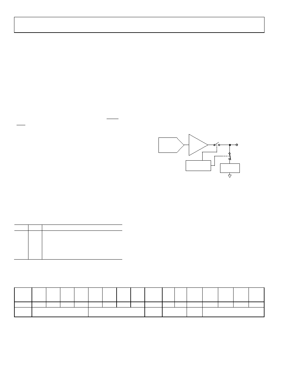
left open-circuited (three-state). The output stage is illustrated in
RESISTOR
NETWORK
VOUT
DAC
POWER-DOWN
CIRCUITRY
AMPLIFIER
06803-
011
Figure 51. Output Stage During Power-Down
The bias generator, output amplifier, resistor string, and other
associated linear circuitry are shut down when the power-down
mode is activated. However, the contents of the DAC register
are unaffected when in power-down. The DAC register can be
updated while the device is in power-down mode. The time to
Table 13. 32-Bit Shift Register Contents for Power-Up/Power-Down Function
MSB
LSB
DB31
to
DB28
DB27
DB26
DB25
DB24
DB23
DB22
DB21
DB20
DB19
to
DB10
DB9
DB8
DB7
to
DB4
DB3
DB2
DB1
DB0
X
0
1
0
X
PD1
PD0
X
DAC D
DAC C
DAC B
DAC A
Don’t
cares
Command bits (C3 to C0)
Address bits (A3 to A0)—
don’t cares
Don’t
cares
Power-
down mode
Don’t
cares
Power-down/power-up channel
selection—set bit to 1 to select
相关PDF资料 |
PDF描述 |
|---|---|
| AD8582AR-REEL | IC DAC DUAL 12BIT 5V 24SOIC |
| AD7225LRZ | IC DAC 8BIT QUAD W/AMP 24SOIC |
| VI-B3Y-MY-B1 | CONVERTER MOD DC/DC 3.3V 33W |
| AD7541AKN | IC DAC 12BIT MULTIPLYING 18-DIP |
| VI-B3Z-MY-B1 | CONVERTER MOD DC/DC 2V 20W |
相关代理商/技术参数 |
参数描述 |
|---|---|
| AD5064BRUZ | 功能描述:IC DAC 16BIT 4CH BUF OUT 16TSSOP RoHS:是 类别:集成电路 (IC) >> 数据采集 - 数模转换器 系列:nanoDAC™ 产品培训模块:Lead (SnPb) Finish for COTS Obsolescence Mitigation Program 标准包装:50 系列:- 设置时间:4µs 位数:12 数据接口:串行 转换器数目:2 电压电源:单电源 功率耗散(最大):- 工作温度:-40°C ~ 85°C 安装类型:表面贴装 封装/外壳:8-TSSOP,8-MSOP(0.118",3.00mm 宽) 供应商设备封装:8-uMAX 包装:管件 输出数目和类型:2 电压,单极 采样率(每秒):* 产品目录页面:1398 (CN2011-ZH PDF) |
| AD5064BRUZ-1 | 功能描述:IC DAC 16BIT 4CH BUF OUT 14TSSOP RoHS:是 类别:集成电路 (IC) >> 数据采集 - 数模转换器 系列:nanoDAC™ 产品培训模块:Lead (SnPb) Finish for COTS Obsolescence Mitigation Program 标准包装:50 系列:- 设置时间:4µs 位数:12 数据接口:串行 转换器数目:2 电压电源:单电源 功率耗散(最大):- 工作温度:-40°C ~ 85°C 安装类型:表面贴装 封装/外壳:8-TSSOP,8-MSOP(0.118",3.00mm 宽) 供应商设备封装:8-uMAX 包装:管件 输出数目和类型:2 电压,单极 采样率(每秒):* 产品目录页面:1398 (CN2011-ZH PDF) |
| AD5064BRUZ-1REEL7 | 功能描述:IC DAC 16BIT 4CH BUF OUT 14TSSOP RoHS:是 类别:集成电路 (IC) >> 数据采集 - 数模转换器 系列:nanoDAC™ 产品培训模块:Data Converter Fundamentals DAC Architectures 标准包装:750 系列:- 设置时间:7µs 位数:16 数据接口:并联 转换器数目:1 电压电源:双 ± 功率耗散(最大):100mW 工作温度:0°C ~ 70°C 安装类型:表面贴装 封装/外壳:28-LCC(J 形引线) 供应商设备封装:28-PLCC(11.51x11.51) 包装:带卷 (TR) 输出数目和类型:1 电压,单极;1 电压,双极 采样率(每秒):143k |
| AD5064BRUZ-REEL7 | 功能描述:IC DAC 16BIT 4CH BUF OUT 16TSSOP RoHS:是 类别:集成电路 (IC) >> 数据采集 - 数模转换器 系列:nanoDAC™ 产品培训模块:Data Converter Fundamentals DAC Architectures 标准包装:750 系列:- 设置时间:7µs 位数:16 数据接口:并联 转换器数目:1 电压电源:双 ± 功率耗散(最大):100mW 工作温度:0°C ~ 70°C 安装类型:表面贴装 封装/外壳:28-LCC(J 形引线) 供应商设备封装:28-PLCC(11.51x11.51) 包装:带卷 (TR) 输出数目和类型:1 电压,单极;1 电压,双极 采样率(每秒):143k |
| AD5065 | 制造商:AD 制造商全称:Analog Devices 功能描述:Fully Accurate, 12-/14-/16-Bit, Dual, VOUT nanoDAC SPI Interface, 4.5 V to 5.5 V in a TSSOP |
发布紧急采购,3分钟左右您将得到回复。