参数资料
| 型号: | AD5170BRM2.5 |
| 厂商: | Analog Devices Inc |
| 文件页数: | 9/24页 |
| 文件大小: | 0K |
| 描述: | IC DGTL POT 2.5K 256POS 10-MSOP |
| 标准包装: | 50 |
| 接片: | 256 |
| 电阻(欧姆): | 2.5k |
| 电路数: | 1 |
| 温度系数: | 标准值 35 ppm/°C |
| 存储器类型: | 易失 |
| 接口: | I²C,2 线串口 |
| 电源电压: | 2.7 V ~ 5.5 V |
| 工作温度: | -40°C ~ 125°C |
| 安装类型: | 表面贴装 |
| 封装/外壳: | 10-TFSOP,10-MSOP(0.118",3.00mm 宽) |
| 供应商设备封装: | 10-MSOP |
| 包装: | 管件 |
AD5170
Rev. G | Page 17 of 24
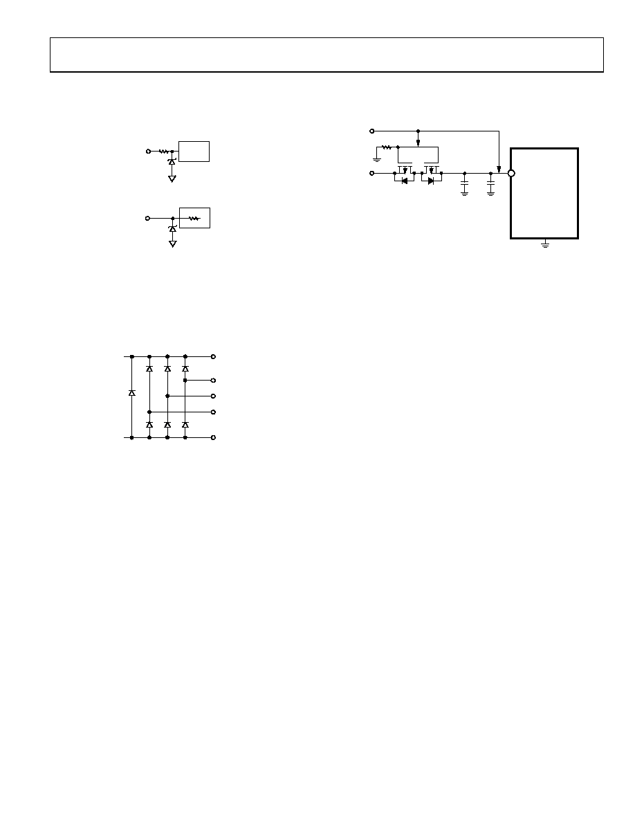
ESD PROTECTION
All digital inputs, SDA, SCL, AD0, and AD1, are protected with
a series input resistor and parallel Zener ESD structures, as shown
LOGIC
340
GND
04
10
4
-03
7
Figure 37. ESD Protection of Digital Pins
A, B, W
GND
04
10
4-
0
38
Figure 38. ESD Protection of Resistor Terminals
TERMINAL VOLTAGE OPERATING RANGE
The AD5170 VDD-to-GND power supply defines the boundary
conditions for proper 3-terminal digital potentiometer opera-
tion. Supply signals present on Terminal A, Terminal B, and
Terminal W that exceed VDD or GND are clamped by the internal
forward-biased diodes (see Figure 39).
GND
A
W
B
VDD
04
10
4-
0
39
Figure 39. Maximum Terminal Voltages Set by VDD and GND
POWER-UP SEQUENCE
Because the ESD protection diodes limit the voltage compliance
at Terminal A, Terminal B, and Terminal W, it is important to
power VDD/GND before applying any voltage to Terminal A,
Terminal B, and Terminal W (see Figure 39). Otherwise, the
diode is forward-biased such that VDD is powered unintentionally
and may affect the rest of the user’s circuit. The ideal power-up
sequence is GND, VDD, the digital inputs, and then VA/VB/VW.
The relative order of powering VA, VB, VW, and the digital inputs
is not important as long as they are powered up after GND/VDD.
POWER SUPPLY CONSIDERATIONS
To minimize the package pin count, both the one-time pro-
gramming and normal operating voltage supplies share the
same VDD terminal of the AD5170. The AD5170 employs fuse
link technology that requires 5.6 V to 5.8 V for blowing the
internal fuses to achieve a given setting, but normal VDD can be
anywhere between 2.7 V and 5.5 V after the fuse programming
process. As a result, dual voltage supplies and isolation are needed if
system VDD is lower than the required VDD_OTP. The fuse program-
ming supply (either an on-board regulator or rack-mount power
supply) must be rated at 5.6 V to 5.8 V and be able to provide a
100 mA current for 400 ms for successful OTP.
When the fuse programming is complete, the VDD_OTP supply
must be removed to allow normal operation at 2.7 V to 5.5 V,
and the device consumes current in the μA range.
VDD
2.7V
5.7V
P1
P1 = P2 = FDV302P, NDS0610
R1
10k
P2
C1
10F
C2
0.1F
APPLY FOR OTP ONLY
AD5170
0
41
04
-0-
51
Figure 40. Isolate 5.7 V OTP Supply from 2.7 V Normal Operating Supply
For example, for those who operate their systems at 2.7 V, use of
the bidirectional, low threshold, P-Channel MOSFETs is recom-
mended for the isolation of the supply. As shown in Figure 40,
this assumes that the 2.7 V system voltage is applied first, and
the P1 and P2 gates are pulled to ground, thus turning on P1 and,
subsequently, P2. As a result, VDD of the AD5170 approaches 2.7 V.
When the AD5170 setting is found, the factory tester applies the
VDD_OTP to both the VDD and the MOSFETs gates, turning off P1
and P2. The OTP command is executed at this time to program the
AD5170 while the 2.7 V source is protected. When the fuse pro-
gramming is complete, the tester withdraws the VDD_OTP and the
setting for the AD5170 is permanently fixed.
The AD5170 achieves the OTP function by blowing internal
fuses. Users should always apply the 5.6 V to 5.8 V one-time-
program voltage requirement at the first fuse programming
attempt. Failure to comply with this requirement can lead to a
change in the fuse structures, rendering programming inoperable.
Care should be taken when SCL and SDA are driven from a low
voltage logic controller. Users must ensure that the logic high
Poor PCB layout introduces parasitics that can affect the fuse
programming. Therefore, it is recommended to add a 10 μF
tantalum capacitor in parallel with a 1 nF ceramic capacitor as
close as possible to the VDD pin. The type and value chosen for
both capacitors are important. This combination of capacitor
values provides both a fast response and larger supply current
handling with minimum supply droop during transients. As a
result, these capacitors increase the OTP programming success
by not inhibiting the proper energy needed to blow the internal
fuses. Additionally, C1 minimizes transient disturbance and low
frequency ripple, and C2 reduces high frequency noise during
normal operation.
相关PDF资料 |
PDF描述 |
|---|---|
| AD5170BRM100 | IC DGTL POT 100K 256POS 10-MSOP |
| VI-24Y-MY-F4 | CONVERTER MOD DC/DC 3.3V 33W |
| VE-25J-MW | CONVERTER MOD DC/DC 36V 100W |
| AD5170BRM10 | IC DGTL POT 10K 256POS 10-MSOP |
| VI-24Y-MY-F2 | CONVERTER MOD DC/DC 3.3V 33W |
相关代理商/技术参数 |
参数描述 |
|---|---|
| AD5170BRM50 | 功能描述:IC DGTL POT 50K 256POS 10-MSOP RoHS:否 类别:集成电路 (IC) >> 数据采集 - 数字电位器 系列:- 标准包装:3,000 系列:DPP 接片:32 电阻(欧姆):10k 电路数:1 温度系数:标准值 300 ppm/°C 存储器类型:非易失 接口:3 线串行(芯片选择,递增,增/减) 电源电压:2.5 V ~ 6 V 工作温度:-40°C ~ 85°C 安装类型:表面贴装 封装/外壳:8-WFDFN 裸露焊盘 供应商设备封装:8-TDFN(2x3) 包装:带卷 (TR) |
| AD5170BRM50-RL7 | 功能描述:IC DGTL POT 50K 256POS 10MSOP TR RoHS:否 类别:集成电路 (IC) >> 数据采集 - 数字电位器 系列:- 标准包装:3,000 系列:DPP 接片:32 电阻(欧姆):10k 电路数:1 温度系数:标准值 300 ppm/°C 存储器类型:非易失 接口:3 线串行(芯片选择,递增,增/减) 电源电压:2.5 V ~ 6 V 工作温度:-40°C ~ 85°C 安装类型:表面贴装 封装/外壳:8-WFDFN 裸露焊盘 供应商设备封装:8-TDFN(2x3) 包装:带卷 (TR) |
| AD5170BRMZ10 | 功能描述:IC POT DGTL 10K 256POS 10-MSOP RoHS:是 类别:集成电路 (IC) >> 数据采集 - 数字电位器 系列:- 标准包装:3,000 系列:DPP 接片:32 电阻(欧姆):10k 电路数:1 温度系数:标准值 300 ppm/°C 存储器类型:非易失 接口:3 线串行(芯片选择,递增,增/减) 电源电压:2.5 V ~ 6 V 工作温度:-40°C ~ 85°C 安装类型:表面贴装 封装/外壳:8-WFDFN 裸露焊盘 供应商设备封装:8-TDFN(2x3) 包装:带卷 (TR) |
| AD5170BRMZ100 | 功能描述:IC POT DGTL 100K 256POS 10-MSOP RoHS:是 类别:集成电路 (IC) >> 数据采集 - 数字电位器 系列:- 标准包装:3,300 系列:WiperLock™ 接片:257 电阻(欧姆):100k 电路数:1 温度系数:标准值 150 ppm/°C 存储器类型:易失 接口:3 线 SPI(芯片选择) 电源电压:1.8 V ~ 5.5 V 工作温度:-40°C ~ 125°C 安装类型:表面贴装 封装/外壳:8-VDFN 裸露焊盘 供应商设备封装:8-DFN-EP(3x3) 包装:带卷 (TR) |
| AD5170BRMZ100-RL7 | 功能描述:IC DGTL POT 256POS 100K 10MSOP RoHS:是 类别:集成电路 (IC) >> 数据采集 - 数字电位器 系列:- 标准包装:3,000 系列:DPP 接片:32 电阻(欧姆):10k 电路数:1 温度系数:标准值 300 ppm/°C 存储器类型:非易失 接口:3 线串行(芯片选择,递增,增/减) 电源电压:2.5 V ~ 6 V 工作温度:-40°C ~ 85°C 安装类型:表面贴装 封装/外壳:8-WFDFN 裸露焊盘 供应商设备封装:8-TDFN(2x3) 包装:带卷 (TR) |
发布紧急采购,3分钟左右您将得到回复。