参数资料
| 型号: | AD5170BRM2.5 |
| 厂商: | Analog Devices Inc |
| 文件页数: | 14/24页 |
| 文件大小: | 0K |
| 描述: | IC DGTL POT 2.5K 256POS 10-MSOP |
| 标准包装: | 50 |
| 接片: | 256 |
| 电阻(欧姆): | 2.5k |
| 电路数: | 1 |
| 温度系数: | 标准值 35 ppm/°C |
| 存储器类型: | 易失 |
| 接口: | I²C,2 线串口 |
| 电源电压: | 2.7 V ~ 5.5 V |
| 工作温度: | -40°C ~ 125°C |
| 安装类型: | 表面贴装 |
| 封装/外壳: | 10-TFSOP,10-MSOP(0.118",3.00mm 宽) |
| 供应商设备封装: | 10-MSOP |
| 包装: | 管件 |
AD5170
Rev. G | Page 21 of 24
I2C CONTROLLER PROGRAMMING
Write Bit Patterns
04
10
4-
04
5
SCL
START BY
MASTER
SDA
01
1
FRAME 1
SLAVE ADDRESS BYTE
0
1
AD1 AD0
FRAME 2
INSTRUCTION BYTE
ACK BY
AD5170
R/W
A0
SD
0
OW XX
X
1
9
D7
D6
D5
D4
D3
ACK BY
AD5170
FRAME 3
DATA BYTE
1
9
T
STOP BY
MASTER
9
D2
D1
D0
ACK BY
AD5170
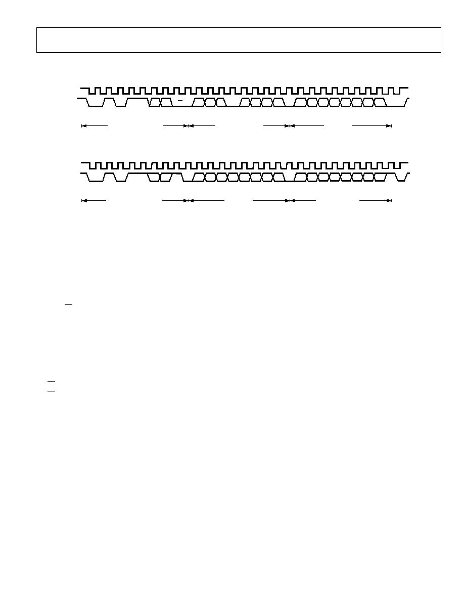
Figure 45. Writing Data to the RDAC Register
Read Bit Pattern
04
10
4-
0
46
SCL
START BY
MASTER
SDA
01
1
FRAME 1
SLAVE ADDRESS BYTE
0
1
AD1 AD0
FRAME 2
DATA BYTE
ACK BY
AD5170
R/W
D7
D6
D4
D3
D2
D1
D0
1
9
E1
E0
X
ACK BY
MASTER
FRAME 3
VALIDATION BYTE
1
9
D5
STOP BY
MASTER
9
XX
X
NO ACK
BY MASTER
Figure 46. Reading Data from the RDAC Register
The third MSB, T, is the OTP programming bit. A logic high
blows the polyfuses and programs the resistor setting perma-
nently. For example, if the user wants to blow the first array
of fuses, the instruction byte is 00100XXX. To blow the second
array of fuses, the instruction byte is 10100XXX. A logic low of
the T bit simply allows the device to act as a typical volatile digital
potentiometer.
I2C-COMPATIBLE, 2-WIRE SERIAL BUS
The following section describes how the 2-wire, I2C serial bus
The master initiates a data transfer by establishing a start con-
dition, which is when a high-to-low transition on the SDA line
occurs while SCL is high (see Figure 45). The following byte is
the slave address byte, which consists of the slave address followed
by an R/W bit (this bit determines whether data is read from or
written to the slave device). AD0 and AD1 are configurable address
bits that allow up to four devices on one bus (see
).
The fourth MSB must always be Logic 0.
The fifth MSB, OW, is an overwrite bit. When raised to a logic
high, OW allows the RDAC setting to be changed even after the
internal fuses are blown. However, when OW is returned to
Logic 0, the position of the RDAC returns to the setting prior to
the overwrite. Because OW is not static, if the device is powered
off and on, the RDAC presets to midscale or to the setting at
which the fuses were blown, depending on whether the fuses
are permanently set.
The slave address corresponding to the transmitted address bits
responds by pulling the SDA line low during the ninth clock
pulse (this is called the acknowledge bit). At this stage, all other
devices on the bus remain idle while the selected device waits
for data to be written to, or read from, its serial register. If the
R/W bit is high, the master reads from the slave device. If the
R/W bit is low, the master writes to the slave device.
The remainder of the bits in the instruction byte are don’t care
bits (see Figure 45).
In write mode, the second byte is the instruction byte. The first
MSB of the instruction byte, 2T, is the second trim enable bit.
A logic low selects the first array of the fuses, and a logic high
selects the second array of the fuses. This means that after blowing
the fuses with Trim 1, the user still has another chance to blow
them again with Trim 2. Note that using Trim 2 before Trim 1
effectively disables Trim 1 and, in turn, allows only one-time
programming.
After acknowledging the instruction byte, the last byte in write
mode is the data byte. Data is transmitted over the serial bus in
sequences of nine clock pulses (eight data bits followed by an
acknowledge bit). The transitions on the SDA line must occur
during the low period of SCL and remain stable during the high
period of SCL (see Figure 2).
In read mode, the data byte follows immediately after the
acknowledgment of the slave address byte. Data is transmitted
over the serial bus in sequences of nine clock pulses (a slight
difference from write mode, with eight data bits followed by an
acknowledge bit). Similarly, transitions on the SDA line must
occur during the low period of SCL and remain stable during
the high period of SCL (see Figure 46).
The second MSB, SD, is a shutdown bit. A logic high causes an
open circuit at Terminal A and shorts the wiper to Terminal B.
This operation yields almost 0 Ω in rheostat mode or 0 V in
potentiometer mode. Note that the shutdown operation does
not disturb the contents of the register. When brought out of
shutdown, the previous setting is applied to the RDAC. In
addition, new settings can be programmed during shutdown.
When the part is returned from shutdown, the corresponding
VR setting is applied to the RDAC.
Following the data byte, the validation byte contains two valida-
tion bits, E0 and E1. These bits signify the status of the one-time
programming (see Figure 46).
相关PDF资料 |
PDF描述 |
|---|---|
| AD5170BRM100 | IC DGTL POT 100K 256POS 10-MSOP |
| VI-24Y-MY-F4 | CONVERTER MOD DC/DC 3.3V 33W |
| VE-25J-MW | CONVERTER MOD DC/DC 36V 100W |
| AD5170BRM10 | IC DGTL POT 10K 256POS 10-MSOP |
| VI-24Y-MY-F2 | CONVERTER MOD DC/DC 3.3V 33W |
相关代理商/技术参数 |
参数描述 |
|---|---|
| AD5170BRM50 | 功能描述:IC DGTL POT 50K 256POS 10-MSOP RoHS:否 类别:集成电路 (IC) >> 数据采集 - 数字电位器 系列:- 标准包装:3,000 系列:DPP 接片:32 电阻(欧姆):10k 电路数:1 温度系数:标准值 300 ppm/°C 存储器类型:非易失 接口:3 线串行(芯片选择,递增,增/减) 电源电压:2.5 V ~ 6 V 工作温度:-40°C ~ 85°C 安装类型:表面贴装 封装/外壳:8-WFDFN 裸露焊盘 供应商设备封装:8-TDFN(2x3) 包装:带卷 (TR) |
| AD5170BRM50-RL7 | 功能描述:IC DGTL POT 50K 256POS 10MSOP TR RoHS:否 类别:集成电路 (IC) >> 数据采集 - 数字电位器 系列:- 标准包装:3,000 系列:DPP 接片:32 电阻(欧姆):10k 电路数:1 温度系数:标准值 300 ppm/°C 存储器类型:非易失 接口:3 线串行(芯片选择,递增,增/减) 电源电压:2.5 V ~ 6 V 工作温度:-40°C ~ 85°C 安装类型:表面贴装 封装/外壳:8-WFDFN 裸露焊盘 供应商设备封装:8-TDFN(2x3) 包装:带卷 (TR) |
| AD5170BRMZ10 | 功能描述:IC POT DGTL 10K 256POS 10-MSOP RoHS:是 类别:集成电路 (IC) >> 数据采集 - 数字电位器 系列:- 标准包装:3,000 系列:DPP 接片:32 电阻(欧姆):10k 电路数:1 温度系数:标准值 300 ppm/°C 存储器类型:非易失 接口:3 线串行(芯片选择,递增,增/减) 电源电压:2.5 V ~ 6 V 工作温度:-40°C ~ 85°C 安装类型:表面贴装 封装/外壳:8-WFDFN 裸露焊盘 供应商设备封装:8-TDFN(2x3) 包装:带卷 (TR) |
| AD5170BRMZ100 | 功能描述:IC POT DGTL 100K 256POS 10-MSOP RoHS:是 类别:集成电路 (IC) >> 数据采集 - 数字电位器 系列:- 标准包装:3,300 系列:WiperLock™ 接片:257 电阻(欧姆):100k 电路数:1 温度系数:标准值 150 ppm/°C 存储器类型:易失 接口:3 线 SPI(芯片选择) 电源电压:1.8 V ~ 5.5 V 工作温度:-40°C ~ 125°C 安装类型:表面贴装 封装/外壳:8-VDFN 裸露焊盘 供应商设备封装:8-DFN-EP(3x3) 包装:带卷 (TR) |
| AD5170BRMZ100-RL7 | 功能描述:IC DGTL POT 256POS 100K 10MSOP RoHS:是 类别:集成电路 (IC) >> 数据采集 - 数字电位器 系列:- 标准包装:3,000 系列:DPP 接片:32 电阻(欧姆):10k 电路数:1 温度系数:标准值 300 ppm/°C 存储器类型:非易失 接口:3 线串行(芯片选择,递增,增/减) 电源电压:2.5 V ~ 6 V 工作温度:-40°C ~ 85°C 安装类型:表面贴装 封装/外壳:8-WFDFN 裸露焊盘 供应商设备封装:8-TDFN(2x3) 包装:带卷 (TR) |
发布紧急采购,3分钟左右您将得到回复。