- 您现在的位置:买卖IC网 > PDF目录9301 > AD5203ARUZ10-REEL (Analog Devices Inc)IC POT DGTL QUAD 64POS 24TSSOP PDF资料下载
参数资料
| 型号: | AD5203ARUZ10-REEL |
| 厂商: | Analog Devices Inc |
| 文件页数: | 2/12页 |
| 文件大小: | 0K |
| 描述: | IC POT DGTL QUAD 64POS 24TSSOP |
| 标准包装: | 2,500 |
| 接片: | 64 |
| 电阻(欧姆): | 10k |
| 电路数: | 4 |
| 温度系数: | 标准值 700 ppm/°C |
| 存储器类型: | 易失 |
| 接口: | 4 线 SPI(芯片选择) |
| 电源电压: | 2.7 V ~ 5.5 V |
| 工作温度: | -40°C ~ 85°C |
| 安装类型: | 表面贴装 |
| 封装/外壳: | 24-TSSOP(0.173",4.40mm 宽) |
| 供应商设备封装: | 24-TSSOP |
| 包装: | 带卷 (TR) |
AD5203
–10–
REV. 0
PROGRAMMING THE POTENTIOMETER DIVIDER
Voltage Output Operation
The digital potentiometer easily generates an output voltage
proportional to the input voltage applied to a given terminal.
For example connecting A–terminal to +5 V and B–terminal to
ground produces an output voltage at the wiper which can be
any value starting at zero volts up to 1 LSB less than +5 V.
Each LSB of voltage is equal to the voltage applied across ter-
minal AB divided by the 64 position resolution of the potenti-
ometer divider. The general equation defining the output
voltage with respect to ground for any given input voltage ap-
plied to terminals AB is:
VW(Dx) = Dx/64
× V
AB + VB
Operation of the digital potentiometer in the divider mode
results in more accurate operation over temperature. Here the
output voltage is dependent on the ratio of the internal resistors
not the absolute value, therefore the drift improves to 20 ppm/
°C.
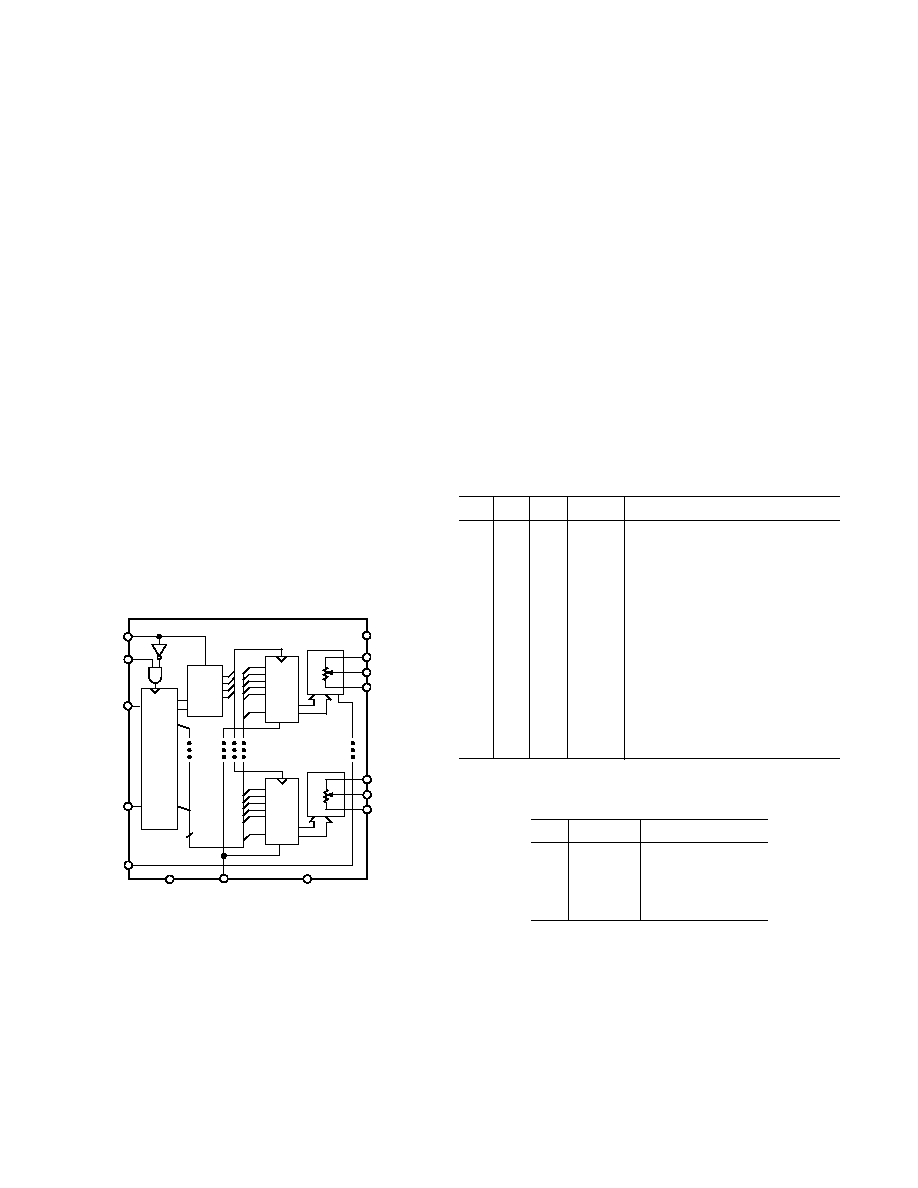
DIGITAL INTERFACING
The AD5203 contains a standard three-wire serial input control
interface. The three inputs are clock (CLK),
CS and serial data
input (SDI). The positive-edge sensitive CLK input requires
clean transitions to avoid clocking incorrect data into the serial
input register. Standard logic families work well. If mechanical
switches are used for product evaluation they should be de-
bounced by a flip-flop or other suitable means. The Figure 35
block diagram shows more detail of the internal digital cir-
cuitry. When
CS is taken active low the clock loads data into
the serial register on each positive clock edge, see Table III.
AGND
A1
W1
B1
VDD
AD5203
CS
CLK
6
D5
D0
EN
ADDR
DEC
A1
A0
SDI
DI
SER
REG
D0
D5
SDO
DO
DGND
A4
W4
B4
SHDN
RS
DAC
LAT
#1
R
D5
D0
DAC
LAT
#4
R
Figure 35. Block Diagram
The serial-data-output (SDO) pin contains an open drain
n-channel FET. This output requires a pull-up resistor in order
to transfer data to the next package’s SDI pin. The pull-up
resistor termination voltage may be larger than the VDD supply
of the AD5203 SDO output device, e.g., the AD5203 could
operate at VDD = 3.3 V and the pull-up for interface to the next
device could be set at +5 V. This allows for daisy chaining sev-
eral RDACs from a single processor serial data line. Clock pe-
riod needs to be increased when using a pull-up resistor to the
SDI pin of the following device in the series. Capacitive loading
at the daisy chain node SDO-SDI between devices must be
accounted for to successfully transfer data. When daisy chaining
is used, the
CS should be kept low until all the bits of every
package are clocked into their respective serial registers insuring
that the address bits and data bits are in the proper decoding
location. This would require 16 bits of address and data comply-
ing to the word format provided in Table I if two AD5203 four-
channel RDACs are daisy chained. During shutdown,
SHDN
the SDO output pin is forced to the off (logic high state) to
disable power dissipation in the pull-up resistor. See Figure 37
for equivalent SDO output circuit schematic.
Table II. Input Logic Control Truth Table
CLK
CS
RS SHDN Register Activity
L
H
No SR effect, enables SDO pin.
P
L
H
Shift one bit in from the SDI pin.
The eighth previously entered bit
is shifted out of the SDO pin.
X
P
H
Load SR data into RDAC latch
based on A1, A0 decode (Table III).
X
H
No Operation.
X
L
H
Sets all RDAC latches to midscale,
wiper centered and SDO latch
cleared.
X
H
P
H
Latches all RDAC latches to 20H.
X
H
L
Open circuits all Resistor A–termi-
nals, connects W to B, turns off
SDO output transistor.
NOTE: P = positive edge, X = don’t care, SR = shift register.
Table III. Address Decode Table
A1
A0
Latch Decoded
0
RDAC#1
0
1
RDAC#2
1
0
RDAC#3
1
RDAC#4
相关PDF资料 |
PDF描述 |
|---|---|
| LTC6994IDCB-2#TRPBF | IC DELAY LINE 6-DFN |
| VI-BNB-IU-F4 | CONVERTER MOD DC/DC 95V 200W |
| LTC6994IDCB-2#TRMPBF | IC DELAY LINE 6-DFN |
| VI-BNB-IU-F3 | CONVERTER MOD DC/DC 95V 200W |
| AD8400ARZ1-REEL | IC POT DGTL 8BIT SGL 1K 8SOIC |
相关代理商/技术参数 |
参数描述 |
|---|---|
| AD5203ARZ10 | 功能描述:IC POT DGTL QUAD 64POS 24SOIC RoHS:是 类别:集成电路 (IC) >> 数据采集 - 数字电位器 系列:- 产品培训模块:Lead (SnPb) Finish for COTS Obsolescence Mitigation Program 标准包装:1 系列:- 接片:256 电阻(欧姆):100k 电路数:1 温度系数:标准值 35 ppm/°C 存储器类型:非易失 接口:3 线串口 电源电压:2.7 V ~ 5.25 V 工作温度:-40°C ~ 85°C 安装类型:表面贴装 封装/外壳:8-WDFN 裸露焊盘 供应商设备封装:8-TDFN-EP(3x3) 包装:剪切带 (CT) 产品目录页面:1399 (CN2011-ZH PDF) 其它名称:MAX5423ETA+TCT |
| AD5203ARZ100 | 功能描述:IC POT DGTL QUAD 64POS 24SOIC RoHS:是 类别:集成电路 (IC) >> 数据采集 - 数字电位器 系列:- 标准包装:2,500 系列:XDCP™ 接片:256 电阻(欧姆):100k 电路数:1 温度系数:标准值 ±300 ppm/°C 存储器类型:非易失 接口:I²C(设备位址) 电源电压:2.7 V ~ 5.5 V 工作温度:0°C ~ 70°C 安装类型:表面贴装 封装/外壳:14-TSSOP(0.173",4.40mm 宽) 供应商设备封装:14-TSSOP 包装:带卷 (TR) |
| AD5203ARZ100-REEL | 功能描述:IC POT DGTL QUAD 64POS 24SOIC RoHS:是 类别:集成电路 (IC) >> 数据采集 - 数字电位器 系列:- 标准包装:3,000 系列:DPP 接片:32 电阻(欧姆):10k 电路数:1 温度系数:标准值 300 ppm/°C 存储器类型:非易失 接口:3 线串行(芯片选择,递增,增/减) 电源电压:2.5 V ~ 6 V 工作温度:-40°C ~ 85°C 安装类型:表面贴装 封装/外壳:8-WFDFN 裸露焊盘 供应商设备封装:8-TDFN(2x3) 包装:带卷 (TR) |
| AD5204 | 制造商:AD 制造商全称:Analog Devices 功能描述:256-Position and 33-Position Digital Potentiometers |
| AD5204_10 | 制造商:AD 制造商全称:Analog Devices 功能描述:4-/6-Channel Digital Potentiometers |
发布紧急采购,3分钟左右您将得到回复。