- 您现在的位置:买卖IC网 > PDF目录9301 > AD5203ARUZ10-REEL (Analog Devices Inc)IC POT DGTL QUAD 64POS 24TSSOP PDF资料下载
参数资料
| 型号: | AD5203ARUZ10-REEL |
| 厂商: | Analog Devices Inc |
| 文件页数: | 6/12页 |
| 文件大小: | 0K |
| 描述: | IC POT DGTL QUAD 64POS 24TSSOP |
| 标准包装: | 2,500 |
| 接片: | 64 |
| 电阻(欧姆): | 10k |
| 电路数: | 4 |
| 温度系数: | 标准值 700 ppm/°C |
| 存储器类型: | 易失 |
| 接口: | 4 线 SPI(芯片选择) |
| 电源电压: | 2.7 V ~ 5.5 V |
| 工作温度: | -40°C ~ 85°C |
| 安装类型: | 表面贴装 |
| 封装/外壳: | 24-TSSOP(0.173",4.40mm 宽) |
| 供应商设备封装: | 24-TSSOP |
| 包装: | 带卷 (TR) |
–3–
REV. 0
AD5203
NOTES
1Typicals represent average readings at +25
°C and V
DD = +5 V.
2Resistor position nonlinearity error R-INL is the deviation from an ideal value measured between the maximum resistance and the minimum resistance wiper posi-
tions. R-DNL measures the relative step change from ideal between successive tap positions. Parts are guaranteed monotonic. See Figure 27 test circuit. I W = VDD/R
for both VDD = +3 V or VDD = +5 V.
3V
AB = VDD, Wiper (VW) = No connect.
4INL and DNL are measured at V
W with the RDAC configured as a potentiometer divider similar to a voltage output D/A converter. V A = VDD and VB = 0 V.
DNL specification limits of
±1 LSB maximum are guaranteed monotonic operating conditions. See Figure 26 test circuit.
5Resistor terminals A, B, W have no limitations on polarity with respect to each other.
6Guaranteed by design and not subject to production test.
7Measured at the AX terminals. All AX terminals are open-circuited in shutdown mode.
8Worst case supply current consumed when all logic-input levels set at 2.4 V, standard characteristic of CMOS logic. See Figure 19 for a plot of I
DD vs. logic voltage
inputs result in minimum power dissipation.
9P
DISS is calculated from (IDD × V DD). CMOS logic level inputs result in minimum power dissipation.
10All dynamic characteristics use V
DD = +5 V.
11Measured at a V
W pin where an adjacent VW pin is making a full-scale voltage change.
12See timing diagrams for location of measured values. All input control voltages are specified with t
R = tF = 1 ns (10% to 90% of VDD) and timed from a voltage level
of 1.6 V. Switching characteristics are measured using both VDD = +3 V or +5 V. Input logic should have a 1 V/ s minimum slew rate.
13Propagation delay depends on value of V
DD, RL and CL. See Operation section.
ABSOLUTE MAXIMUM RATINGS*
(TA = +25°C, unless otherwise noted)
VDD to GND . . . . . . . . . . . . . . . . . . . . . . . . . . . . –0.3 V, +8 V
VA, VB, VW to GND . . . . . . . . . . . . . . . . . . . . . . . . . . 0 V, VDD
IAB, IAW, IBW . . . . . . . . . . . . . . . . . . . . . . . . . . . . . . .
±20 mA
Digital Input and Output Voltage to GND . . . . . . . 0 V, +8 V
Operating Temperature Range . . . . . . . . . . . –40
°C to +85°C
Maximum Junction Temperature (TJ MAX) . . . . . . . . +150
°C
Storage Temperature . . . . . . . . . . . . . . . . . . –65
°C to +150°C
Lead Temperature (Soldering, 10 sec) . . . . . . . . . . . . +300
°C
Package Power Dissipation . . . . . . . . . . . . . . (TJ max–TA)/
θ
JA
Thermal Resistance
θ
JA
P-DIP (N-24) . . . . . . . . . . . . . . . . . . . . . . . . . . . . 63
°C/W
SOIC (SOL-24) . . . . . . . . . . . . . . . . . . . . . . . . . . . 70
°C/W
TSSOP-24 . . . . . . . . . . . . . . . . . . . . . . . . . . . . . . 143
°C/W
*Stresses above those listed under Absolute Maximum Ratings may cause perma-
nent damage to the device. This is a stress rating only; functional operation of the
device at these or any other conditions above those indicated in the operational
sections of this specification is not implied. Exposure to absolute maximum rating
conditions for extended periods may affect device reliability.
Table I. Serial-Data Word Format
ADDR
DATA
B7
B6
B5
B4
B3
B2
B1
B0
A1
A0
D5
D4
D3
D2
D1
D0
MSB
LSB
MSB
LSB
27
26
25
20
CAUTION
ESD (electrostatic discharge) sensitive device. Electrostatic charges as high as 4000 V readily
accumulate on the human body and test equipment and can discharge without detection.
Although the AD5203 features proprietary ESD protection circuitry, permanent damage may
occur on devices subjected to high energy electrostatic discharges. Therefore, proper ESD
precautions are recommended to avoid performance degradation or loss of functionality.
WARNING!
ESD SENSITIVE DEVICE
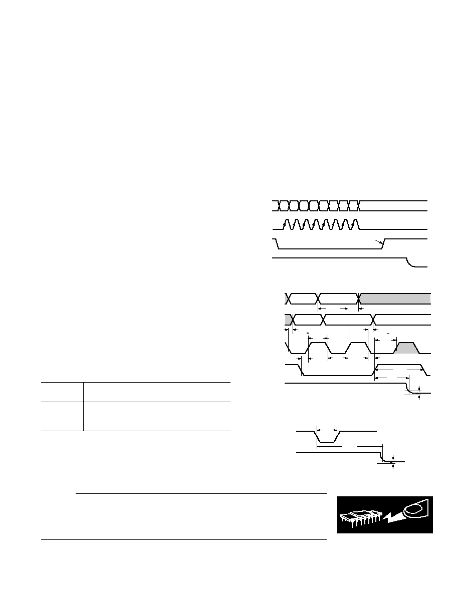
SDI
CLK
CS
VOUT
1
0
1
0
1
0
VDD
0V
D0
D1
D2
D3
D4
D5
A0
A1
DAC REGISTER LOAD
Figure 1a. Timing Diagram
CLK
VOUT
1
0
1
0
1
0
VDD
0V
SDI
(DATA IN)
SDO
(DATA OUT)
CS
1
0
Ax OR Dx
A'x OR D'x
tDS
tDH
tPD MAX
tPD MIN
tCH
tCS1
tCL
tCSS
tCSH
1 LSB
1 LSB ERROR BAND
tCSW
tS
A'x OR D'x
Figure 1b. Detail Timing Diagram
VOUT
VDD
0V
RS
1
0
1 LSB
1 LSB ERROR BAND
tS
tRS
Figure 1c. Reset Timing Diagram
相关PDF资料 |
PDF描述 |
|---|---|
| LTC6994IDCB-2#TRPBF | IC DELAY LINE 6-DFN |
| VI-BNB-IU-F4 | CONVERTER MOD DC/DC 95V 200W |
| LTC6994IDCB-2#TRMPBF | IC DELAY LINE 6-DFN |
| VI-BNB-IU-F3 | CONVERTER MOD DC/DC 95V 200W |
| AD8400ARZ1-REEL | IC POT DGTL 8BIT SGL 1K 8SOIC |
相关代理商/技术参数 |
参数描述 |
|---|---|
| AD5203ARZ10 | 功能描述:IC POT DGTL QUAD 64POS 24SOIC RoHS:是 类别:集成电路 (IC) >> 数据采集 - 数字电位器 系列:- 产品培训模块:Lead (SnPb) Finish for COTS Obsolescence Mitigation Program 标准包装:1 系列:- 接片:256 电阻(欧姆):100k 电路数:1 温度系数:标准值 35 ppm/°C 存储器类型:非易失 接口:3 线串口 电源电压:2.7 V ~ 5.25 V 工作温度:-40°C ~ 85°C 安装类型:表面贴装 封装/外壳:8-WDFN 裸露焊盘 供应商设备封装:8-TDFN-EP(3x3) 包装:剪切带 (CT) 产品目录页面:1399 (CN2011-ZH PDF) 其它名称:MAX5423ETA+TCT |
| AD5203ARZ100 | 功能描述:IC POT DGTL QUAD 64POS 24SOIC RoHS:是 类别:集成电路 (IC) >> 数据采集 - 数字电位器 系列:- 标准包装:2,500 系列:XDCP™ 接片:256 电阻(欧姆):100k 电路数:1 温度系数:标准值 ±300 ppm/°C 存储器类型:非易失 接口:I²C(设备位址) 电源电压:2.7 V ~ 5.5 V 工作温度:0°C ~ 70°C 安装类型:表面贴装 封装/外壳:14-TSSOP(0.173",4.40mm 宽) 供应商设备封装:14-TSSOP 包装:带卷 (TR) |
| AD5203ARZ100-REEL | 功能描述:IC POT DGTL QUAD 64POS 24SOIC RoHS:是 类别:集成电路 (IC) >> 数据采集 - 数字电位器 系列:- 标准包装:3,000 系列:DPP 接片:32 电阻(欧姆):10k 电路数:1 温度系数:标准值 300 ppm/°C 存储器类型:非易失 接口:3 线串行(芯片选择,递增,增/减) 电源电压:2.5 V ~ 6 V 工作温度:-40°C ~ 85°C 安装类型:表面贴装 封装/外壳:8-WFDFN 裸露焊盘 供应商设备封装:8-TDFN(2x3) 包装:带卷 (TR) |
| AD5204 | 制造商:AD 制造商全称:Analog Devices 功能描述:256-Position and 33-Position Digital Potentiometers |
| AD5204_10 | 制造商:AD 制造商全称:Analog Devices 功能描述:4-/6-Channel Digital Potentiometers |
发布紧急采购,3分钟左右您将得到回复。