- 您现在的位置:买卖IC网 > PDF目录9288 > AD5233BRUZ10-R7 (Analog Devices Inc)IC DGTL POT QUAD 64POS 24-TSSOP PDF资料下载
参数资料
| 型号: | AD5233BRUZ10-R7 |
| 厂商: | Analog Devices Inc |
| 文件页数: | 13/32页 |
| 文件大小: | 0K |
| 描述: | IC DGTL POT QUAD 64POS 24-TSSOP |
| 标准包装: | 1,000 |
| 接片: | 64 |
| 电阻(欧姆): | 10k |
| 电路数: | 4 |
| 温度系数: | 标准值 600 ppm/°C |
| 存储器类型: | 非易失 |
| 接口: | 4 线 SPI(芯片选择) |
| 电源电压: | 2.7 V ~ 5.5 V,±2.25 V ~ 2.75 V |
| 工作温度: | -40°C ~ 85°C |
| 安装类型: | 表面贴装 |
| 封装/外壳: | 24-TSSOP(0.173",4.40mm 宽) |
| 供应商设备封装: | 24-TSSOP |
| 包装: | 带卷 (TR) |
第1页第2页第3页第4页第5页第6页第7页第8页第9页第10页第11页第12页当前第13页第14页第15页第16页第17页第18页第19页第20页第21页第22页第23页第24页第25页第26页第27页第28页第29页第30页第31页第32页
AD5233
Rev. B | Page 20 of 32
Using Additional Internal Nonvolatile EEMEM
The AD5233 contains additional user EEMEM registers for
storing any 8-bit data. Table 9 provides an address map of the
internal storage registers shown in the functional block diagram
as EEMEM1, EEMEM2, and 11 bytes of user EEMEM.
Table 9. EEMEM Address Map
EEMEM Number
Address
EEMEM Content
1
0000
RDAC11, 2
2
0001
RDAC21, 2
3
0010
RDAC31, 2
4
0011
RDAC41, 2
5
0100
O1 and O23
6
0101
7
0110
USER2
…
15
1110
USER10
16
1111
USER11
1 RDAC data stored in the EEMEM location is transferred to the RDAC register
at power-on, or when Instruction 1, Instruction 8, and PR are executed.
2 Execution of Instruction 1 leaves the device in the read mode power
consumption state. After the last Instruction 1 is executed, the user
should perform a NOP, Instruction 0, to return the device to the low
power idling state.
3 O1 and O2 data stored in EEMEM locations is transferred to the corresponding
digital register at power-on, or when Instruction 1 and Instruction 8 are
executed.
4 USERx are internal nonvolatile EEMEM registers available to store and
retrieve constants and other 8-bit information using Instruction 3 and
Instruction 9, respectively.
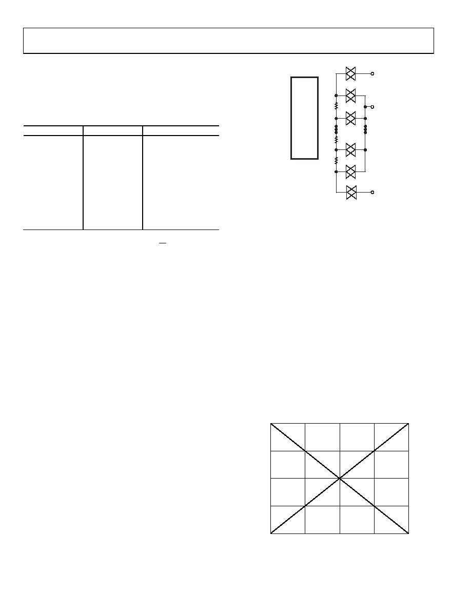
RDAC STRUCTURE
The patent-pending RDAC contains multiple strings of equal
resistor segments, with an array of analog switches that act as
the wiper connection. The number of positions is the resolution
of the device. The AD5233 has 64 connection points, allowing it
to provide better than 1.5% set ability resolution. Figure 43
shows an equivalent structure of the connections between the
three terminals of the RDAC. The SWA and SWB are always on,
while the switches, SW(0) to SW(2N1), are on, one at a time,
depending on the resistance position decoded from the data
bits. Because the switch is not ideal, there is a 15 Ω wiper
resistance, RW. Wiper resistance is a function of supply voltage
and temperature. The lower the supply voltage or the higher the
temperature, the higher the resulting wiper resistance. Users
should be aware of the wiper resistance dynamics if an accurate
prediction of the output resistance is needed.
SW(1)
SW(0)
SWB
B
SWA
SW(2N – 1)
SW(2N – 2)
A
W
RDAC
WIPER
REGISTER
AND
DECODER
RS = RAB/2N
RS
DIGITAL
CIRCUITRY
OMITTED FOR
CLARITY
0
27
94
-04
4
Figure 43. Equivalent RDAC Structure
PROGRAMMING THE VARIABLE RESISTOR
Rheostat Operation
The nominal resistance of the RDAC between Terminal A
and Terminal B, RAB, is available with 10 kΩ, 50 kΩ, and 100 kΩ
with 64 positions (6-bit resolution). The final digit(s) of the part
number determine the nominal resistance value, for example,
10 = 10 kΩ; 50 = 50 kΩ; 100 = 100 kΩ.
The 6-bit data-word in the RDAC latch is decoded to select
one of the 64 possible settings. The following discussion
describes the calculation of resistance (RWB) at different codes
of a 10 kΩ part. For VDD = 5 V, the wiper’s first connection
starts at Terminal B for Data 0x00. RWB(0) is 15 Ω because of
the wiper resistance and because it is independent of the nominal
resistance. The second connection is the first tap point, where
RWB(1) becomes 156 Ω + 15 Ω = 171 Ω for Data 0x01. The third
connection is the next tap point, representing RWB(2) = 321 Ω +
15 Ω = 327 Ω for Data 0x02, and so on. Each LSB data value
increase moves the wiper up the resistor ladder until the last
simplified diagram of the equivalent RDAC circuit. When RWB
is used, Terminal A can be left floating or tied to the wiper.
CODE (Decimal)
100
75
0
06
16
R
WA
(D
),
4
R
WB
(D
)(
%
o
fF
u
ll
-S
ca
le
R
AB
)
32
48
50
25
RWB
RWA
0
27
94
-04
5
Figure 44. RWA(D) and RWB(D) vs. Decimal Code
相关PDF资料 |
PDF描述 |
|---|---|
| MS27484E16F35SD | CONN PLUG 55POS STRAIGHT W/SCKT |
| DS1100LZ-30+T | IC DELAY LINE 5TAP 30NS 8-SOIC |
| VI-B4Z-MW-F1 | CONVERTER MOD DC/DC 2V 40W |
| VI-B4Y-MY-F1 | CONVERTER MOD DC/DC 3.3V 33W |
| DS1100LZ-50+T | IC DELAY LINE 5TAP 50NS 8-SOIC |
相关代理商/技术参数 |
参数描述 |
|---|---|
| AD5233BRUZ50 | 功能描述:IC POT QUAD 50K 64POS 24-TSSOP RoHS:是 类别:集成电路 (IC) >> 数据采集 - 数字电位器 系列:- 产品培训模块:Lead (SnPb) Finish for COTS Obsolescence Mitigation Program 标准包装:1 系列:- 接片:256 电阻(欧姆):100k 电路数:1 温度系数:标准值 35 ppm/°C 存储器类型:非易失 接口:3 线串口 电源电压:2.7 V ~ 5.25 V 工作温度:-40°C ~ 85°C 安装类型:表面贴装 封装/外壳:8-WDFN 裸露焊盘 供应商设备封装:8-TDFN-EP(3x3) 包装:剪切带 (CT) 产品目录页面:1399 (CN2011-ZH PDF) 其它名称:MAX5423ETA+TCT |
| AD5233BRUZ50-R7 | 功能描述:IC DGTL POT QUAD 64POS 24-TSSOP RoHS:是 类别:集成电路 (IC) >> 数据采集 - 数字电位器 系列:- 标准包装:3,000 系列:DPP 接片:32 电阻(欧姆):10k 电路数:1 温度系数:标准值 300 ppm/°C 存储器类型:非易失 接口:3 线串行(芯片选择,递增,增/减) 电源电压:2.5 V ~ 6 V 工作温度:-40°C ~ 85°C 安装类型:表面贴装 封装/外壳:8-WFDFN 裸露焊盘 供应商设备封装:8-TDFN(2x3) 包装:带卷 (TR) |
| AD5235 | 制造商:AD 制造商全称:Analog Devices 功能描述:8-Bit Dual Nonvolatile Memory Digital Potentiometer |
| AD5235BRU25 | 制造商:Analog Devices 功能描述:Digital Potentiometer 1024POS 25KOhm Dual 16-Pin TSSOP 制造商:Analog Devices 功能描述:IC DIGITAL POT 25KOHM 1024 DUAL 16-TSSO |
| AD5235BRU250 | 制造商:Analog Devices 功能描述:Digital Potentiometer 1024POS 250KOhm Dual 16-Pin TSSOP 制造商:Analog Devices 功能描述:IC DUAL DIGITAL POT. 10-BIT |
发布紧急采购,3分钟左右您将得到回复。