- 您现在的位置:买卖IC网 > PDF目录9288 > AD5233BRUZ10-R7 (Analog Devices Inc)IC DGTL POT QUAD 64POS 24-TSSOP PDF资料下载
参数资料
| 型号: | AD5233BRUZ10-R7 |
| 厂商: | Analog Devices Inc |
| 文件页数: | 16/32页 |
| 文件大小: | 0K |
| 描述: | IC DGTL POT QUAD 64POS 24-TSSOP |
| 标准包装: | 1,000 |
| 接片: | 64 |
| 电阻(欧姆): | 10k |
| 电路数: | 4 |
| 温度系数: | 标准值 600 ppm/°C |
| 存储器类型: | 非易失 |
| 接口: | 4 线 SPI(芯片选择) |
| 电源电压: | 2.7 V ~ 5.5 V,±2.25 V ~ 2.75 V |
| 工作温度: | -40°C ~ 85°C |
| 安装类型: | 表面贴装 |
| 封装/外壳: | 24-TSSOP(0.173",4.40mm 宽) |
| 供应商设备封装: | 24-TSSOP |
| 包装: | 带卷 (TR) |
第1页第2页第3页第4页第5页第6页第7页第8页第9页第10页第11页第12页第13页第14页第15页当前第16页第17页第18页第19页第20页第21页第22页第23页第24页第25页第26页第27页第28页第29页第30页第31页第32页
AD5233
Rev. B | Page 23 of 32
APPLICATIONS INFORMATION
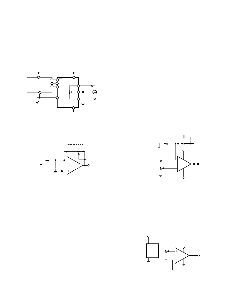
BIPOLAR OPERATION FROM DUAL SUPPLIES
The AD5233 can be operated from dual supplies ±2.5 V, which
enables control of ground-referenced ac signals or bipolar opera-
tion. AC signals as high as VDD/VSS can be applied directly
across Terminal A and Terminal B with output taken from
Terminal W. See Figure 46 for a typical circuit connection.
±2.5V p-p
AD5233
VSS
GND
SDI
CLK
SS
SCLK
MOSI
GND
MICRO-
CONVERTER
±1.25V p-p
VDD
+2.5V
–2.5V
CS
D = MIDSCALE
A
W
B
02
79
4
-04
7
Figure 46. Bipolar Operation from Dual Supplies
GAIN CONTROL COMPENSATION
A digital potentiometer is commonly used in gain control such
as the noninverting gain amplifier shown in Figure 47.
U1
VO
R2
100k
Vi
R1
33.2k
C1
35pF
W
BA
C2
10pF
02
79
4-
04
8
Figure 47. Typical Noninverting Gain Amplifier
When RDAC B terminal parasitic capacitance is connected
to the op amp noninverting node, it introduces a 0 for the
1/bO term with 20 dB/dec, while a typical op amp GBP has
20 dB/dec characteristics. A large R2 and finite C1 can cause
this zero’s frequency to fall well below the crossover frequency.
Therefore, the rate of closure becomes 40 dB/dec, and the
system as a 0° phase margin at the crossover frequency. The
output can ring or oscillate if an input is a rectangular pulse or
step function. Similarly, it is also likely to ring when switching
between two gain values; this is equivalent to a stop change at
the input.
Depending on the op amp GBP, reducing the feedback
resistor might extend the zero’s frequency far enough to
overcome the problem. A better approach is to include a
compensation capacitor, C2, to cancel the effect caused by
C1. Optimum compensation occurs when R1 × C1 = R2 ×
C2. This is not an option because of the variation of R2.
As a result, one can use the previous relationship and scale C2
as if R2 were at its maximum value. Doing this might over-
compensate and compromise the performance when R2 is
set at low values. On the other hand, it avoids the ringing or
oscillation at the worst case. For critical applications, C2 should
be found empirically to suit the need. In general, C2 in the
range of picofarads is usually adequate for the compensation.
Similarly, W and A terminal capacitances are connected to the
output (not shown); their effect at this node is less significant
and the compensation can be avoided in most cases.
HIGH VOLTAGE OPERATION
The digital potentiometer can be placed directly in the feedback
or input path of an op amp for gain control, provided that the
voltage across Terminal A and Terminal B, Terminal W and
Terminal A, or Terminal W and Terminal B does not exceed
|5 V|. When high voltage gain is needed, users should set a
fixed gain in an op amp operated at high voltage and let the
digital potentiometer control the adjustable input. Figure 48
shows a simple implementation.
R2R
5V
AD5233
A
W
B
15V
V+
V–
VO
0 TO 15V
A2
–
+
C
0
27
94
-0
49
Figure 48. 5 V Voltage Span Control
Similarly, a compensation capacitor, C, might be needed to
dampen the potential ringing when the digital potentiometer
changes steps. This effect is prominent when stray capacitance
at the inverted node is augmented by a large feedback resistor.
Usually, a capacitor (C) of a few picofarads, is adequate to combat
the problem.
DAC
Figure 49 shows a unipolar 8-bit DAC using the AD5233. The
buffer is needed to drive various loads.
AD5233
V+
V–
AD8601
W
A1
VIN VOUT
GND
AD1582
5V
U1
3
A
B
VO
1
2
02
79
4-
05
0
Figure 49. Unipolar 8-Bit DAC
相关PDF资料 |
PDF描述 |
|---|---|
| MS27484E16F35SD | CONN PLUG 55POS STRAIGHT W/SCKT |
| DS1100LZ-30+T | IC DELAY LINE 5TAP 30NS 8-SOIC |
| VI-B4Z-MW-F1 | CONVERTER MOD DC/DC 2V 40W |
| VI-B4Y-MY-F1 | CONVERTER MOD DC/DC 3.3V 33W |
| DS1100LZ-50+T | IC DELAY LINE 5TAP 50NS 8-SOIC |
相关代理商/技术参数 |
参数描述 |
|---|---|
| AD5233BRUZ50 | 功能描述:IC POT QUAD 50K 64POS 24-TSSOP RoHS:是 类别:集成电路 (IC) >> 数据采集 - 数字电位器 系列:- 产品培训模块:Lead (SnPb) Finish for COTS Obsolescence Mitigation Program 标准包装:1 系列:- 接片:256 电阻(欧姆):100k 电路数:1 温度系数:标准值 35 ppm/°C 存储器类型:非易失 接口:3 线串口 电源电压:2.7 V ~ 5.25 V 工作温度:-40°C ~ 85°C 安装类型:表面贴装 封装/外壳:8-WDFN 裸露焊盘 供应商设备封装:8-TDFN-EP(3x3) 包装:剪切带 (CT) 产品目录页面:1399 (CN2011-ZH PDF) 其它名称:MAX5423ETA+TCT |
| AD5233BRUZ50-R7 | 功能描述:IC DGTL POT QUAD 64POS 24-TSSOP RoHS:是 类别:集成电路 (IC) >> 数据采集 - 数字电位器 系列:- 标准包装:3,000 系列:DPP 接片:32 电阻(欧姆):10k 电路数:1 温度系数:标准值 300 ppm/°C 存储器类型:非易失 接口:3 线串行(芯片选择,递增,增/减) 电源电压:2.5 V ~ 6 V 工作温度:-40°C ~ 85°C 安装类型:表面贴装 封装/外壳:8-WFDFN 裸露焊盘 供应商设备封装:8-TDFN(2x3) 包装:带卷 (TR) |
| AD5235 | 制造商:AD 制造商全称:Analog Devices 功能描述:8-Bit Dual Nonvolatile Memory Digital Potentiometer |
| AD5235BRU25 | 制造商:Analog Devices 功能描述:Digital Potentiometer 1024POS 25KOhm Dual 16-Pin TSSOP 制造商:Analog Devices 功能描述:IC DIGITAL POT 25KOHM 1024 DUAL 16-TSSO |
| AD5235BRU250 | 制造商:Analog Devices 功能描述:Digital Potentiometer 1024POS 250KOhm Dual 16-Pin TSSOP 制造商:Analog Devices 功能描述:IC DUAL DIGITAL POT. 10-BIT |
发布紧急采购,3分钟左右您将得到回复。