- 您现在的位置:买卖IC网 > PDF目录373873 > AD5245BRJ50-RL7 (ANALOG DEVICES INC) 256-Position I2C Compatible Digital Potentiometer PDF资料下载
参数资料
| 型号: | AD5245BRJ50-RL7 |
| 厂商: | ANALOG DEVICES INC |
| 元件分类: | 数字电位计 |
| 英文描述: | 256-Position I2C Compatible Digital Potentiometer |
| 中文描述: | 50K DIGITAL POTENTIOMETER, 2-WIRE SERIAL CONTROL INTERFACE, 256 POSITIONS, PDSO8 |
| 封装: | 2.90 X 3 MM, MO-178BA, SOT-23, 8 PIN |
| 文件页数: | 14/16页 |
| 文件大小: | 995K |
| 代理商: | AD5245BRJ50-RL7 |
AD5245
A repeated write function gives the user flexibility to update the
RDAC output a number of times after addressing and
instructing the part only once. During the write cycle, each data
byte will update the RDAC output. For example, after the RDAC
has acknowledged its slave address and instruction bytes, the
RDAC output will update after these two bytes. If another byte
is written to the RDAC while it is still addressed to a specific
slave device with the same instruction, this byte will update the
output of the selected slave device. If different instructions are
needed, the write mode has to start again with a new slave
address, instruction, and data byte. Similarly, a repeated read
function of the RDAC is also allowed.
Readback RDAC Value
The AD5245 allows the user to read back the RDAC values in
the read mode. Refer to Table 5 and Table 6 for the
programming format.
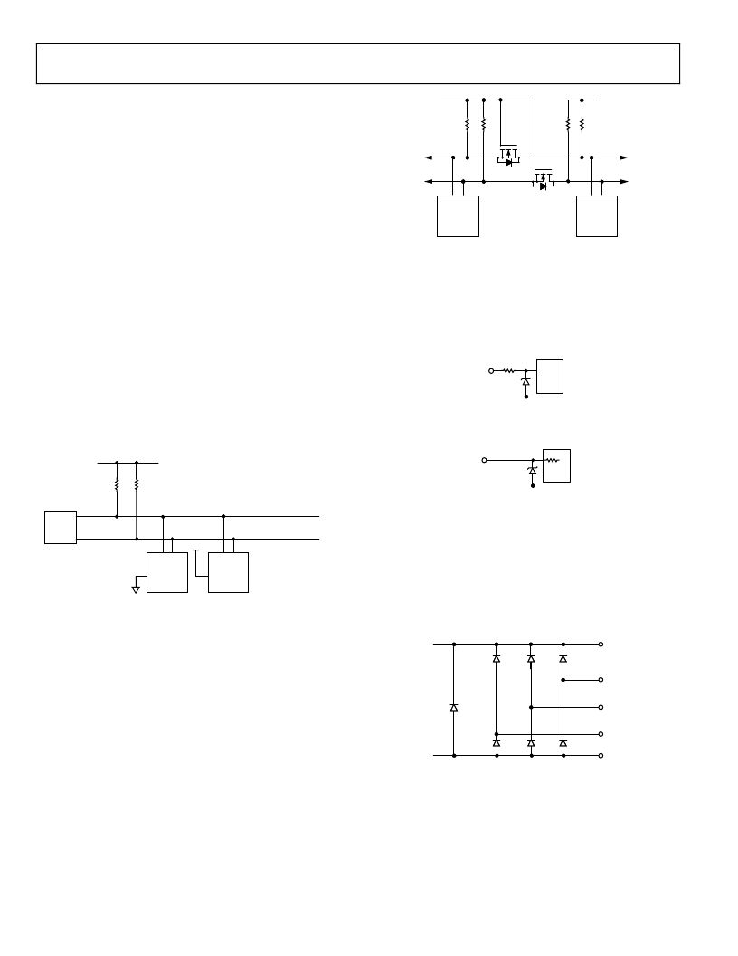
Multiple Devices on One Bus
Figure 40 shows two AD5245 devices on the same serial bus.
Each has a different slave address since the states of their AD0
pins are different. This allows each RDAC within each device to
be written to or read from independently. The master device
output bus line drivers are open-drain pull-downs in a fully I
2
C
compatible interface.
MASTER
AD5245
SDA SCL
R
P
R
P
+5V
+5V
SDA
SCL
SDA SCL
AD5245
AD0
AD0
Figure 40. Multiple AD5245 Devices on One I
2
C Bus
LEVEL SHIFTING FOR BIDIRECTIONAL INTERFACE
While most legacy systems may be operated at one voltage, a
new component may be optimized at another. When two
systems operate the same signal at two different voltages, proper
level shifting is needed. For instance, one can use a 3.3 V
E
2
PROM to interface with a 5 V digital potentiometer. A level
shifting scheme is needed to enable a bidirectional
communication so that the setting of the digital potentiometer
can be stored to and retrieved from the E
2
PROM. Figure 41
shows one of the implementations. M1 and M2 can be any
N-channel signal FETs, or if V
DD
falls below 2.5 V, low threshold
FETs such as the FDV301N.
E
2
PROM
AD5245
SDA1
SCL1
D
G
R
P
R
P
3.3V
5V
S
M1
SCL2
SDA2
R
P
R
P
G
S
M2
V
DD1
= 3.3V
V
DD2=
5V
D
Figure 41. Level Shifting for Operation at Different Potentials
ESD PROTECTION
All digital inputs are protected with a series input resistor and
parallel Zener ESD structures shown in Figure 42 and Figure 43.
This applies to the digital input pins SDA, SCL, and AD0.
LOGIC
340
V
SS
Figure 42. ESD Protection of Digital Pins
A,B,W
V
SS
Figure 43. ESD Protection of Resistor Terminals
TERMINAL VOLTAGE OPERATING RANGE
The AD5245 V
DD
and GND power supply defines the boundary
conditions for proper 3-terminal digital potentiometer
operation. Supply signals present on terminals A, B, and W that
exceed V
DD
or GND will be clamped by the internal forward
biased diodes (see Figure 44).
A
V
DD
B
W
V
SS
Figure 44. Maximum Terminal Voltages Set by V
DD
and V
SS
Rev. 0 | Page 14 of 16
相关PDF资料 |
PDF描述 |
|---|---|
| AD5245EVAL | 256-Position I2C Compatible Digital Potentiometer |
| AD5246 | 128-Position I2C Compatible Digital Resistor |
| AD5246BKS10-R2 | 128-Position I2C Compatible Digital Resistor |
| AD5246BKS10-RL7 | 128-Position I2C Compatible Digital Resistor |
| AD5246BKS100-R2 | 128-Position I2C Compatible Digital Resistor |
相关代理商/技术参数 |
参数描述 |
|---|---|
| AD5245BRJ5-R2 | 制造商:Analog Devices 功能描述:IC DIGITAL POT. 8-BIT I2C |
| AD5245BRJ5-RL7 | 制造商:Analog Devices 功能描述:Digital Potentiometer 256POS 5KOhm Single 8-Pin SOT-23 T/R |
| AD5245BRJZ100 | 制造商:Analog Devices 功能描述:DGTL POT 256POS 100K SOT23-8 制造商:Analog Devices 功能描述:DGTL POT, 256POS, 100K, SOT23-8 |
| AD5245BRJZ100-R2 | 功能描述:IC DGTL POT 256POS SOT-23-8 T/R RoHS:是 类别:集成电路 (IC) >> 数据采集 - 数字电位器 系列:- 标准包装:3,000 系列:DPP 接片:32 电阻(欧姆):10k 电路数:1 温度系数:标准值 300 ppm/°C 存储器类型:非易失 接口:3 线串行(芯片选择,递增,增/减) 电源电压:2.5 V ~ 6 V 工作温度:-40°C ~ 85°C 安装类型:表面贴装 封装/外壳:8-WFDFN 裸露焊盘 供应商设备封装:8-TDFN(2x3) 包装:带卷 (TR) |
| AD5245BRJZ100-R21 | 制造商:AD 制造商全称:Analog Devices 功能描述:256-Position I2C-Compatible Digital Potentiometer |
发布紧急采购,3分钟左右您将得到回复。