- 您现在的位置:买卖IC网 > PDF目录9293 > AD5252BRU1-RL7 (Analog Devices Inc)IC DCP DUAL 1K 256POS 14TSSOP TR PDF资料下载
参数资料
| 型号: | AD5252BRU1-RL7 |
| 厂商: | Analog Devices Inc |
| 文件页数: | 16/28页 |
| 文件大小: | 0K |
| 描述: | IC DCP DUAL 1K 256POS 14TSSOP TR |
| 标准包装: | 1,000 |
| 接片: | 256 |
| 电阻(欧姆): | 1k |
| 电路数: | 2 |
| 温度系数: | 标准值 650 ppm/°C |
| 存储器类型: | 非易失 |
| 接口: | I²C(设备位址) |
| 电源电压: | 2.7 V ~ 5.5 V,±2.25 V ~ 2.75 V |
| 工作温度: | -40°C ~ 85°C |
| 安装类型: | 表面贴装 |
| 封装/外壳: | 14-TSSOP(0.173",4.40mm 宽) |
| 供应商设备封装: | 14-TSSOP |
| 包装: | 带卷 (TR) |
第1页第2页第3页第4页第5页第6页第7页第8页第9页第10页第11页第12页第13页第14页第15页当前第16页第17页第18页第19页第20页第21页第22页第23页第24页第25页第26页第27页第28页
Data Sheet
AD5251/AD5252
Rev. D | Page 23 of 28
LAYOUT AND POWER SUPPLY BIASING
It is always a good practice to employ a compact, minimum
lead-length layout design. The leads to the input should be as
direct as possible, with a minimum conductor length. Ground
paths should have low resistance and low inductance.
Similarly, it is also good practice to bypass the power supplies
with quality capacitors. Low equivalent series resistance (ESR)
1 μF to 10 μF tantalum or electrolytic capacitors should be
applied at the supplies to minimize any transient disturbance
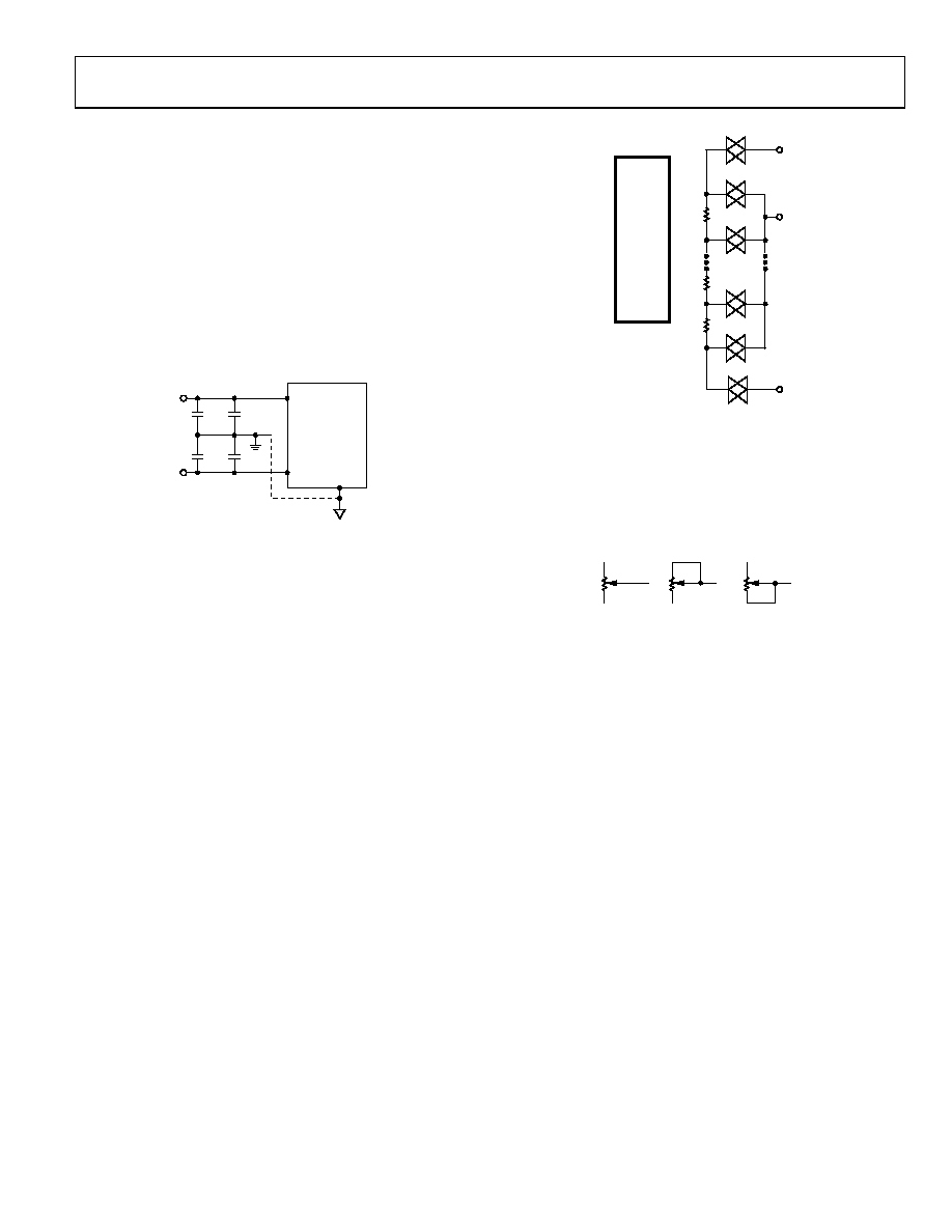
and filter low frequency ripple. Figure 39 illustrates the basic
supply-bypassing configuration for the AD5251/AD5252.
VDD
VSS
GND
C3
AD5251/AD5252
C4
C1
+
C2
10
F
10
F
0.1
F
0.1
F
03823-0-039
Figure 39. Power Supply-Bypassing Configuration
The ground pin of the AD5251/AD5252 is used primarily as a
digital ground reference. To minimize the digital ground
bounce, the AD5251/AD5252 ground terminal should be joined
remotely to the common ground (see Figure 39).
DIGITAL POTENTIOMETER OPERATION
The structure of the RDAC is designed to emulate the
performance of a mechanical potentiometer. The RDAC
contains a string of resistor segments with an array of analog
switches that act as the wiper connection to the resistor array.
The number of points is the resolution of the device. For
example, the AD5251/AD5252 emulate 64/256 connection
points with 64/256 equal resistance, RS, allowing them to
provide better than 1.5%/0.4% resolution.
Figure 40 provides an equivalent diagram of the connections
between the three terminals that make up one channel of the
RDAC. Switches SWA and SWB are always on, but only one of
switches SW(0) to SW(2N – 1) can be on at a time (determined by
the setting decoded from the data bit). Because the switches are
nonideal, there is a 75 Ω wiper resistance, RW. Wiper resistance
is a function of supply voltage and temperature: Lower supply
voltages and higher temperatures result in higher wiper
resistances. Consideration of wiper resistance dynamics is
important in applications in which accurate prediction of
output resistance is required.
SWB
SW(1)
SW(0)
BX
RS
SWA
SW(2N – 1)
AX
WX
SW(2N – 2)
RDAC
WIPER
REGISTER
AND
DECODER
RS = RAB/2N
RS
DIGITAL
CIRCUITRY
OMITTED FOR
CLARITY
03823-0-040
Figure 40. Equivalent RDAC Structure
PROGRAMMABLE RHEOSTAT OPERATION
If either the W-to-B or W-to-A terminal is used as a variable
resistor, the unused terminal can be opened or shorted with W;
such operation is called rheostat mode (see Figure 41). The
resistance tolerance can range ±20%.
A
W
B
03823-0-041
A
W
B
A
W
B
Figure 41. Rheostat Mode Configuration
The nominal resistance of the AD5251/AD5252 has 64/256
contact points accessed by the wiper terminal, plus the B terminal
contact. The 6-/8-bit data-word in the RDAC register is decoded
to select one of the 64/256 settings. The wiper’s first connection
starts at the B terminal for Data 0x00. This B terminal connection
has a wiper contact resistance, RW, of 75 Ω, regardless of the
nominal resistance. The second connection (the AD5251 10 kΩ
part) is the first tap point where RWB = 231 Ω (RWB = RAB/64 +
RW = 156 Ω + 75 Ω) for Data 0x01, and so on. Each LSB data
value increase moves the wiper up the resistor ladder until the
simplified diagram of the equivalent RDAC circuit.
The general equation that determines the digitally programmed
output resistance between W and B is
AD5251: RWB(D) = (D/64) × RAB + 75 Ω
(1)
AD5252: RWB(D) = (D/256) × RAB + 75 Ω
(2)
where:
D is the decimal equivalent of the data contained in the
RDAC latch.
RAB is the nominal end-to-end resistance.
相关PDF资料 |
PDF描述 |
|---|---|
| VI-263-MY-F3 | CONVERTER MOD DC/DC 24V 50W |
| DS1100Z-45+ | IC DELAY LINE 5TAP 45NS 8-SOIC |
| DS1100Z-45 | IC DELAY LINE 5TAP 45NS 8-SOIC |
| AD5207BRU100 | IC DGTL POT DUAL 256POS 14TSSOP |
| VI-263-MY-F1 | CONVERTER MOD DC/DC 24V 50W |
相关代理商/技术参数 |
参数描述 |
|---|---|
| AD5252BRU50 | 功能描述:IC DCP DUAL 50K 256POS 14TSSOP RoHS:否 类别:集成电路 (IC) >> 数据采集 - 数字电位器 系列:- 标准包装:3,000 系列:DPP 接片:32 电阻(欧姆):10k 电路数:1 温度系数:标准值 300 ppm/°C 存储器类型:非易失 接口:3 线串行(芯片选择,递增,增/减) 电源电压:2.5 V ~ 6 V 工作温度:-40°C ~ 85°C 安装类型:表面贴装 封装/外壳:8-WFDFN 裸露焊盘 供应商设备封装:8-TDFN(2x3) 包装:带卷 (TR) |
| AD5252BRU50-RL7 | 功能描述:IC DCP DUAL 50K 256POS 14TSSOP RoHS:否 类别:集成电路 (IC) >> 数据采集 - 数字电位器 系列:- 标准包装:3,000 系列:DPP 接片:32 电阻(欧姆):10k 电路数:1 温度系数:标准值 300 ppm/°C 存储器类型:非易失 接口:3 线串行(芯片选择,递增,增/减) 电源电压:2.5 V ~ 6 V 工作温度:-40°C ~ 85°C 安装类型:表面贴装 封装/外壳:8-WFDFN 裸露焊盘 供应商设备封装:8-TDFN(2x3) 包装:带卷 (TR) |
| AD5252BRUZ1 | 功能描述:IC DGTL POT DUAL 1K I2C 14-TSSOP RoHS:是 类别:集成电路 (IC) >> 数据采集 - 数字电位器 系列:- 产品培训模块:Lead (SnPb) Finish for COTS Obsolescence Mitigation Program 标准包装:1 系列:- 接片:256 电阻(欧姆):100k 电路数:1 温度系数:标准值 35 ppm/°C 存储器类型:非易失 接口:3 线串口 电源电压:2.7 V ~ 5.25 V 工作温度:-40°C ~ 85°C 安装类型:表面贴装 封装/外壳:8-WDFN 裸露焊盘 供应商设备封装:8-TDFN-EP(3x3) 包装:剪切带 (CT) 产品目录页面:1399 (CN2011-ZH PDF) 其它名称:MAX5423ETA+TCT |
| AD5252BRUZ10 | 功能描述:IC DIG POT DUAL 256 10K 14TSSOP RoHS:是 类别:集成电路 (IC) >> 数据采集 - 数字电位器 系列:- 产品培训模块:Lead (SnPb) Finish for COTS Obsolescence Mitigation Program 标准包装:1 系列:- 接片:256 电阻(欧姆):100k 电路数:1 温度系数:标准值 35 ppm/°C 存储器类型:非易失 接口:3 线串口 电源电压:2.7 V ~ 5.25 V 工作温度:-40°C ~ 85°C 安装类型:表面贴装 封装/外壳:8-WDFN 裸露焊盘 供应商设备封装:8-TDFN-EP(3x3) 包装:剪切带 (CT) 产品目录页面:1399 (CN2011-ZH PDF) 其它名称:MAX5423ETA+TCT |
| AD5252BRUZ100 | 功能描述:IC DIG POT DUAL 256 100K 14TSSOP RoHS:是 类别:集成电路 (IC) >> 数据采集 - 数字电位器 系列:- 产品培训模块:Lead (SnPb) Finish for COTS Obsolescence Mitigation Program 标准包装:1 系列:- 接片:256 电阻(欧姆):100k 电路数:1 温度系数:标准值 35 ppm/°C 存储器类型:非易失 接口:3 线串口 电源电压:2.7 V ~ 5.25 V 工作温度:-40°C ~ 85°C 安装类型:表面贴装 封装/外壳:8-WDFN 裸露焊盘 供应商设备封装:8-TDFN-EP(3x3) 包装:剪切带 (CT) 产品目录页面:1399 (CN2011-ZH PDF) 其它名称:MAX5423ETA+TCT |
发布紧急采购,3分钟左右您将得到回复。