- 您现在的位置:买卖IC网 > PDF目录9308 > AD5274BCPZ-20-RL7 (Analog Devices Inc)IC RHEOSTAT 5V 50-TP 256 10MSOP PDF资料下载
参数资料
| 型号: | AD5274BCPZ-20-RL7 |
| 厂商: | Analog Devices Inc |
| 文件页数: | 17/28页 |
| 文件大小: | 0K |
| 描述: | IC RHEOSTAT 5V 50-TP 256 10MSOP |
| 标准包装: | 1 |
| 接片: | 256 |
| 电阻(欧姆): | 20k |
| 电路数: | 1 |
| 温度系数: | 标准值 5 ppm/°C |
| 存储器类型: | 非易失 |
| 接口: | I²C |
| 电源电压: | 2.7 V ~ 5.5 V,±2.5 V ~ 2.75 V |
| 工作温度: | -40°C ~ 125°C |
| 安装类型: | 表面贴装 |
| 封装/外壳: | 10-TFSOP,10-MSOP(0.118",3.00mm 宽) |
| 供应商设备封装: | 10-MSOP |
| 包装: | 标准包装 |
| 其它名称: | AD5274BCPZ-20-RL7DKR |
第1页第2页第3页第4页第5页第6页第7页第8页第9页第10页第11页第12页第13页第14页第15页第16页当前第17页第18页第19页第20页第21页第22页第23页第24页第25页第26页第27页第28页
AD5272/AD5274
Data Sheet
Rev. D | Page 24 of 28
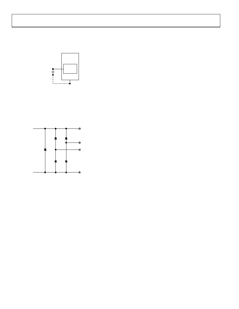
EXT_CAP CAPACITOR
A 1 μF capacitor to VSS must be connected to the EXT_CAP pin
(see Figure 47) on power-up and throughout the operation of
the AD5272/AD5274.
AD5272/
AD5274
50_OTP
MEMORY
BLOCK
EXT_CAP
C1
1F
VSS
08
076
-00
9
Figure 47. EXT_CAP Hardware Setup
TERMINAL VOLTAGE OPERATING RANGE
The positive VDD and negative VSS power supplies of the
AD5272/AD5274 define the boundary conditions for proper
2-terminal digital resistor operation. Supply signals present on
Terminal A and Terminal W that exceed VDD or VSS are clamped
by the internal forward-biased diodes (see Figure 48).
VSS
VDD
A
W
08
076
-10
9
Figure 48. Maximum Terminal Voltages Set by VDD and VSS
The ground pins of the AD5272/AD5274 devices are primarily
used as digital ground references. To minimize the digital
ground bounce, join the AD5272/AD5274 ground terminal
remotely to the common ground. The digital input control
signals to the AD5272/AD5274 must be referenced to the
device ground pin (GND) and satisfy the logic level defined in
the Specifications section. An internal level shift circuit ensures
that the common-mode voltage range of the three terminals
extends from VSS to VDD, regardless of the digital input level.
POWER-UP SEQUENCE
Because there are diodes to limit the voltage compliance at
Terminal A and Terminal W (see Figure 48), it is important to
power VDD/VSS first before applying any voltage to Terminal A
and Terminal W; otherwise, the diode is forward-biased such
that VDD/VSS are powered unintentionally. The ideal power-up
sequence is VSS, GND, VDD, digital inputs, VA, and VW. The
order of powering VA, VW, and digital inputs is not important
as long as they are powered after VDD/VSS.
As soon as VDD is powered, the power-on preset activates, which
first sets the RDAC to midscale and then restores the last
programmed 50-TP value to the RDAC register.
相关PDF资料 |
PDF描述 |
|---|---|
| VE-26J-MY-F2 | CONVERTER MOD DC/DC 36V 50W |
| VE-BNF-IU-F1 | CONVERTER MOD DC/DC 72V 200W |
| VI-2WM-MW | CONVERTER MOD DC/DC 10V 100W |
| VE-26J-MY-F1 | CONVERTER MOD DC/DC 36V 50W |
| VI-2WL-MX-B1 | CONVERTER MOD DC/DC 28V 75W |
相关代理商/技术参数 |
参数描述 |
|---|---|
| AD5274BRMZ-100 | 功能描述:IC RHEOSTAT 5V 50TP 256 10MSOP RoHS:是 类别:集成电路 (IC) >> 数据采集 - 数字电位器 系列:- 产品培训模块:Lead (SnPb) Finish for COTS Obsolescence Mitigation Program 标准包装:1 系列:- 接片:256 电阻(欧姆):100k 电路数:1 温度系数:标准值 35 ppm/°C 存储器类型:非易失 接口:3 线串口 电源电压:2.7 V ~ 5.25 V 工作温度:-40°C ~ 85°C 安装类型:表面贴装 封装/外壳:8-WDFN 裸露焊盘 供应商设备封装:8-TDFN-EP(3x3) 包装:剪切带 (CT) 产品目录页面:1399 (CN2011-ZH PDF) 其它名称:MAX5423ETA+TCT |
| AD5274BRMZ-100-RL7 | 功能描述:IC RHEOSTAT 5V 50-TP 256 10MSOP RoHS:是 类别:集成电路 (IC) >> 数据采集 - 数字电位器 系列:- 标准包装:3,000 系列:DPP 接片:32 电阻(欧姆):10k 电路数:1 温度系数:标准值 300 ppm/°C 存储器类型:非易失 接口:3 线串行(芯片选择,递增,增/减) 电源电压:2.5 V ~ 6 V 工作温度:-40°C ~ 85°C 安装类型:表面贴装 封装/外壳:8-WFDFN 裸露焊盘 供应商设备封装:8-TDFN(2x3) 包装:带卷 (TR) |
| AD5274BRMZ-20 | 功能描述:IC DGTL POT 20K 256POS 10MSOP RoHS:是 类别:集成电路 (IC) >> 数据采集 - 数字电位器 系列:- 产品培训模块:Lead (SnPb) Finish for COTS Obsolescence Mitigation Program 标准包装:1 系列:- 接片:256 电阻(欧姆):100k 电路数:1 温度系数:标准值 35 ppm/°C 存储器类型:非易失 接口:3 线串口 电源电压:2.7 V ~ 5.25 V 工作温度:-40°C ~ 85°C 安装类型:表面贴装 封装/外壳:8-WDFN 裸露焊盘 供应商设备封装:8-TDFN-EP(3x3) 包装:剪切带 (CT) 产品目录页面:1399 (CN2011-ZH PDF) 其它名称:MAX5423ETA+TCT |
| AD5274BRMZ-20 | 制造商:Analog Devices 功能描述:Digital Potentiometer IC |
| AD5274BRMZ-20-RL7 | 功能描述:IC DGTL POT 20K 256POS 10MSOP RoHS:是 类别:集成电路 (IC) >> 数据采集 - 数字电位器 系列:- 标准包装:3,000 系列:DPP 接片:32 电阻(欧姆):10k 电路数:1 温度系数:标准值 300 ppm/°C 存储器类型:非易失 接口:3 线串行(芯片选择,递增,增/减) 电源电压:2.5 V ~ 6 V 工作温度:-40°C ~ 85°C 安装类型:表面贴装 封装/外壳:8-WFDFN 裸露焊盘 供应商设备封装:8-TDFN(2x3) 包装:带卷 (TR) |
发布紧急采购,3分钟左右您将得到回复。