参数资料
| 型号: | AD5312ARMZ |
| 厂商: | Analog Devices Inc |
| 文件页数: | 10/24页 |
| 文件大小: | 0K |
| 描述: | IC DAC 10BIT DUAL R-R 10-MSOP |
| 产品培训模块: | Data Converter Fundamentals DAC Architectures |
| 标准包装: | 50 |
| 设置时间: | 6µs |
| 位数: | 10 |
| 数据接口: | 串行 |
| 转换器数目: | 2 |
| 电压电源: | 单电源 |
| 功率耗散(最大): | 2.5mW |
| 工作温度: | -40°C ~ 105°C |
| 安装类型: | 表面贴装 |
| 封装/外壳: | 10-TFSOP,10-MSOP(0.118",3.00mm 宽) |
| 供应商设备封装: | 10-MSOP |
| 包装: | 管件 |
| 输出数目和类型: | 2 电压,单极;2 电压,双极 |
| 采样率(每秒): | 143k |
| 产品目录页面: | 782 (CN2011-ZH PDF) |
AD5302/AD5312/AD5322
Rev. D | Page 18 of 24
APPLICATIONS INFORMATION
TYPICAL APPLICATION CIRCUIT
The AD5302/AD5312/AD5322 can be used with a wide range
of reference voltages, especially if the reference inputs are
configured to be unbuffered, in which case the devices offer full,
one-quadrant multiplying capability over a reference range of
0 V to VDD. More typically, the AD5302/AD5312/AD5322 can
be used with a fixed, precision reference voltage. Figure 38
shows a typical setup for the AD5302/AD5312/AD5322
when using an external reference. If the reference inputs are
unbuffered, the reference input range is from 0 V to VDD, but if
the on-chip reference buffers are used, the reference range is
reduced. Suitable references for 5 V operation are the AD780
and REF192 (2.5 V references). For 2.5 V operation, a suitable
external reference would be the REF191, a 2.048 V reference.
SCLK
DIN
GND
AD5302/AD5312/
AD5322
SERIAL
INTERFACE
EXT
REF
00
92
8-
03
8
AD780/REF192
WITH VDD = 5V
OR REF191 WITH
VDD = 2.5V
VOUT
SYNC
VOUTA
VOUTB
VREFA
VREFB
1F
VDD = 2.5V to 5.5V
VDD
Figure 38. AD5302/AD5312/AD5322 Using External Reference
If an output range of 0 V to VDD is required when the reference
inputs are configured as unbuffered (for example, 0 V to 5 V),
the simplest solution is to connect the reference inputs to VDD.
As this supply cannot be very accurate and can be noisy, the
AD5302/AD5312/AD5322 can be powered from the reference
voltage, for example, a 5 V reference such as the REF195, as
shown in Figure 39. The REF195 outputs a steady supply
voltage for the AD5302/AD5312/AD5322. The current required
from the REF195 is 300 μA supply current and approximately
30 μA into each reference input. This is with no load on the
DAC outputs. When the DAC outputs are loaded, the REF195
also needs to supply the current to the loads. The total current
required (with a 10 kΩ load on each output) is
mA
36
.
1
k
10
V
5
2
μA
360
=
Ω
+
The load regulation of the REF195 is typically 2 ppm/mA,
which results in an error of 2.7 ppm (13.5 μV) for the 1.36 mA
current drawn from it. This corresponds to a 0.0007 LSB error
at eight bits and a 0.011 LSB error at 12 bits.
SCLK
DIN
GND
AD5302/AD5312/
AD5322
SERIAL
INTERFACE
REF195
00
92
8-
03
9
VOUT
SYNC
VOUTA
VOUTB
VDD
VREFA
1F
6V to 16V
GND
VIN
VREFB
0.1F
10F
Figure 39. Using a REF195 as Power and Reference to the
AD5302/AD5312/AD5322
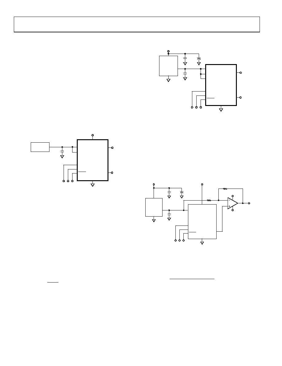
BIPOLAR OPERATION USING THE
AD5302/AD5312/AD5322
The AD5302/AD5312/AD5322 are designed for single-supply
operation, but bipolar operation is also achievable using the
circuit shown in Figure 40. This circuit is configured to achieve
an output voltage range of –5 V < VOUT < +5 V. Rail-to-rail
operation at the amplifier output is achievable using an AD820
or OP295 as the output amplifier.
SCLK
DIN
GND
AD5302/AD5312/
AD5322
SERIAL
INTERFACE
REF195
009
28-
0
40
VOUT
SYNC
VOUTA/B
VREFA/B
1F
GND
VIN
6V to 16V
0.1F
10F
VDD
VDD = 5V
+5V
–5V
R2
10k
AD820/
OP295
R1
10k
±5V
Figure 40. Bipolar Operation Using the AD5302/AD5312/AD5322
The output voltage for any input code can be calculated as
follows:
(
) ()
()
1
/
2
1
2
1
2
/
R
V
R
D
V
REF
N
REF
OUT
×
+
×
=
where:
D is the decimal equivalent of the code loaded to the DAC.
N is the DAC resolution.
VREF is the reference voltage input.
If VREF = 5 V, R1 = R2 = 1 kΩ, and VDD = 5 V:
(
) V
5
2
/
10
×
=
N
OUT
D
V
相关PDF资料 |
PDF描述 |
|---|---|
| VI-J5W-MZ-F2 | CONVERTER MOD DC/DC 5.5V 25W |
| MS3126F22-21SW | CONN PLUG 21POS STRAIGHT W/SCKT |
| MS3126F22-21S | CONN PLUG 21POS STRAIGHT W/SCKT |
| VI-J5W-MZ-F1 | CONVERTER MOD DC/DC 5.5V 25W |
| LTC1329CS8-50#PBF | IC D/A CONV 8BIT MICROPWR 8-SOIC |
相关代理商/技术参数 |
参数描述 |
|---|---|
| AD5312ARMZ-REEL7 | 功能描述:IC DAC 10BIT DUAL R-R 10-MSOP RoHS:是 类别:集成电路 (IC) >> 数据采集 - 数模转换器 系列:- 产品培训模块:Data Converter Fundamentals DAC Architectures 设计资源:Unipolar, Precision DC Digital-to-Analog Conversion using AD5450/1/2/3 8-14-Bit DACs (CN0052) Precision, Bipolar, Configuration for AD5450/1/2/3 8-14bit Multiplying DACs (CN0053) AC Signal Processing Using AD5450/1/2/3 Current Output DACs (CN0054) Programmable Gain Element Using AD5450/1/2/3 Current Output DAC Family (CN0055) Single Supply Low Noise LED Current Source Driver Using a Current Output DAC in the Reverse Mode (CN0139) 标准包装:10,000 系列:- 设置时间:- 位数:12 数据接口:DSP,MICROWIRE?,QSPI?,串行,SPI? 转换器数目:1 电压电源:单电源 功率耗散(最大):- 工作温度:-40°C ~ 125°C 安装类型:表面贴装 封装/外壳:SOT-23-8 薄型,TSOT-23-8 供应商设备封装:TSOT-23-8 包装:带卷 (TR) 输出数目和类型:1 电流,单极;1 电流,双极 采样率(每秒):2.7M |
| AD5312BRM | 功能描述:IC DAC 10BIT DUAL R-R OUT 10MSOP RoHS:否 类别:集成电路 (IC) >> 数据采集 - 数模转换器 系列:- 标准包装:2,400 系列:- 设置时间:- 位数:18 数据接口:串行 转换器数目:3 电压电源:模拟和数字 功率耗散(最大):- 工作温度:-40°C ~ 85°C 安装类型:表面贴装 封装/外壳:36-TFBGA 供应商设备封装:36-TFBGA 包装:带卷 (TR) 输出数目和类型:* 采样率(每秒):* |
| AD5312BRM-REEL | 功能描述:IC DAC 10BIT DUAL W/BUFF 10-MSOP RoHS:否 类别:集成电路 (IC) >> 数据采集 - 数模转换器 系列:- 标准包装:2,400 系列:- 设置时间:- 位数:18 数据接口:串行 转换器数目:3 电压电源:模拟和数字 功率耗散(最大):- 工作温度:-40°C ~ 85°C 安装类型:表面贴装 封装/外壳:36-TFBGA 供应商设备封装:36-TFBGA 包装:带卷 (TR) 输出数目和类型:* 采样率(每秒):* |
| AD5312BRM-REEL7 | 功能描述:IC DAC 10BIT DUAL W/BUFF 10-MSOP RoHS:否 类别:集成电路 (IC) >> 数据采集 - 数模转换器 系列:- 产品培训模块:LTC263x 12-, 10-, and 8-Bit VOUT DAC Family 特色产品:LTC2636 - Octal 12-/10-/8-Bit SPI VOUT DACs with 10ppm/°C Reference 标准包装:91 系列:- 设置时间:4µs 位数:10 数据接口:MICROWIRE?,串行,SPI? 转换器数目:8 电压电源:单电源 功率耗散(最大):2.7mW 工作温度:-40°C ~ 85°C 安装类型:表面贴装 封装/外壳:14-WFDFN 裸露焊盘 供应商设备封装:14-DFN-EP(4x3) 包装:管件 输出数目和类型:8 电压,单极 采样率(每秒):* |
| AD5312BRMZ | 功能描述:IC DAC 10BIT DUAL R-R 10-MSOP RoHS:是 类别:集成电路 (IC) >> 数据采集 - 数模转换器 系列:- 产品培训模块:Lead (SnPb) Finish for COTS Obsolescence Mitigation Program 标准包装:50 系列:- 设置时间:4µs 位数:12 数据接口:串行 转换器数目:2 电压电源:单电源 功率耗散(最大):- 工作温度:-40°C ~ 85°C 安装类型:表面贴装 封装/外壳:8-TSSOP,8-MSOP(0.118",3.00mm 宽) 供应商设备封装:8-uMAX 包装:管件 输出数目和类型:2 电压,单极 采样率(每秒):* 产品目录页面:1398 (CN2011-ZH PDF) |
发布紧急采购,3分钟左右您将得到回复。