参数资料
| 型号: | AD5312ARMZ |
| 厂商: | Analog Devices Inc |
| 文件页数: | 8/24页 |
| 文件大小: | 0K |
| 描述: | IC DAC 10BIT DUAL R-R 10-MSOP |
| 产品培训模块: | Data Converter Fundamentals DAC Architectures |
| 标准包装: | 50 |
| 设置时间: | 6µs |
| 位数: | 10 |
| 数据接口: | 串行 |
| 转换器数目: | 2 |
| 电压电源: | 单电源 |
| 功率耗散(最大): | 2.5mW |
| 工作温度: | -40°C ~ 105°C |
| 安装类型: | 表面贴装 |
| 封装/外壳: | 10-TFSOP,10-MSOP(0.118",3.00mm 宽) |
| 供应商设备封装: | 10-MSOP |
| 包装: | 管件 |
| 输出数目和类型: | 2 电压,单极;2 电压,双极 |
| 采样率(每秒): | 143k |
| 产品目录页面: | 782 (CN2011-ZH PDF) |
AD5302/AD5312/AD5322
Rev. D | Page 16 of 24
POWER-DOWN MODES
The AD5302/AD5312/AD5322 have very low power consump-
tion, dissipating only 0.7 mW with a 3 V supply and 1.5 mW
with a 5 V supply. Power consumption can be further reduced
when the DACs are not in use by putting them into one of three
power-down modes, which are selected by Bit 13 and Bit 12
(PD1 and PD0) of the control word. Table 7 shows how the
state of the bits corresponds to the mode of operation of that
particular DAC.
Table 7. PD1/PD0 Operating Modes
PD1
PDO
Operating Mode
0
Normal Operation
0
1
Power-Down (1 kΩ Load to GND)
1
0
Power-Down (100 kΩ Load to GND)
1
Power-Down (High Impedance Output)
When both bits are set to 0, the DACs work normally with
their normal power consumption of 300 μA at 5 V. However,
for the three power-down modes, the supply current falls to
200 nA at 5 V (50 nA at 3 V). Not only does the supply current
drop, but the output stage is also internally switched from the
output of the amplifier to a resistor network of known values.
This has the advantage that the output impedance of the part is
known while the part is in power-down mode and provides a
defined input condition for whatever is connected to the output
of the DAC amplifier. There are three different options.
The output is connected internally to GND through a
1 kΩ resistor,
The output is connected internally to GND through a
100 kΩ resistor, or
The output is left open-circuited (three-state).
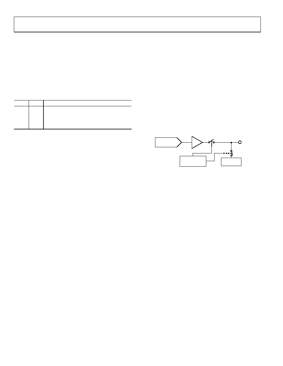
The output stage is illustrated in Figure 33.
The bias generator, the output amplifier, the resistor string,
and all other associated linear circuitry are shut down when
the power-down mode is activated. However, the contents of
the registers are unaffected when in power-down. The time to
exit power-down is typically 2.5 μs for VDD = 5 V and 5 μs when
RESISTOR-
STRING DAC
AMPLIFIER
VOUT
00
92
8-
03
3
POWER-DOWN
CIRCUITRY
RESISTOR
NETWORK
Figure 33. Output Stage During Power-Down
相关PDF资料 |
PDF描述 |
|---|---|
| VI-J5W-MZ-F2 | CONVERTER MOD DC/DC 5.5V 25W |
| MS3126F22-21SW | CONN PLUG 21POS STRAIGHT W/SCKT |
| MS3126F22-21S | CONN PLUG 21POS STRAIGHT W/SCKT |
| VI-J5W-MZ-F1 | CONVERTER MOD DC/DC 5.5V 25W |
| LTC1329CS8-50#PBF | IC D/A CONV 8BIT MICROPWR 8-SOIC |
相关代理商/技术参数 |
参数描述 |
|---|---|
| AD5312ARMZ-REEL7 | 功能描述:IC DAC 10BIT DUAL R-R 10-MSOP RoHS:是 类别:集成电路 (IC) >> 数据采集 - 数模转换器 系列:- 产品培训模块:Data Converter Fundamentals DAC Architectures 设计资源:Unipolar, Precision DC Digital-to-Analog Conversion using AD5450/1/2/3 8-14-Bit DACs (CN0052) Precision, Bipolar, Configuration for AD5450/1/2/3 8-14bit Multiplying DACs (CN0053) AC Signal Processing Using AD5450/1/2/3 Current Output DACs (CN0054) Programmable Gain Element Using AD5450/1/2/3 Current Output DAC Family (CN0055) Single Supply Low Noise LED Current Source Driver Using a Current Output DAC in the Reverse Mode (CN0139) 标准包装:10,000 系列:- 设置时间:- 位数:12 数据接口:DSP,MICROWIRE?,QSPI?,串行,SPI? 转换器数目:1 电压电源:单电源 功率耗散(最大):- 工作温度:-40°C ~ 125°C 安装类型:表面贴装 封装/外壳:SOT-23-8 薄型,TSOT-23-8 供应商设备封装:TSOT-23-8 包装:带卷 (TR) 输出数目和类型:1 电流,单极;1 电流,双极 采样率(每秒):2.7M |
| AD5312BRM | 功能描述:IC DAC 10BIT DUAL R-R OUT 10MSOP RoHS:否 类别:集成电路 (IC) >> 数据采集 - 数模转换器 系列:- 标准包装:2,400 系列:- 设置时间:- 位数:18 数据接口:串行 转换器数目:3 电压电源:模拟和数字 功率耗散(最大):- 工作温度:-40°C ~ 85°C 安装类型:表面贴装 封装/外壳:36-TFBGA 供应商设备封装:36-TFBGA 包装:带卷 (TR) 输出数目和类型:* 采样率(每秒):* |
| AD5312BRM-REEL | 功能描述:IC DAC 10BIT DUAL W/BUFF 10-MSOP RoHS:否 类别:集成电路 (IC) >> 数据采集 - 数模转换器 系列:- 标准包装:2,400 系列:- 设置时间:- 位数:18 数据接口:串行 转换器数目:3 电压电源:模拟和数字 功率耗散(最大):- 工作温度:-40°C ~ 85°C 安装类型:表面贴装 封装/外壳:36-TFBGA 供应商设备封装:36-TFBGA 包装:带卷 (TR) 输出数目和类型:* 采样率(每秒):* |
| AD5312BRM-REEL7 | 功能描述:IC DAC 10BIT DUAL W/BUFF 10-MSOP RoHS:否 类别:集成电路 (IC) >> 数据采集 - 数模转换器 系列:- 产品培训模块:LTC263x 12-, 10-, and 8-Bit VOUT DAC Family 特色产品:LTC2636 - Octal 12-/10-/8-Bit SPI VOUT DACs with 10ppm/°C Reference 标准包装:91 系列:- 设置时间:4µs 位数:10 数据接口:MICROWIRE?,串行,SPI? 转换器数目:8 电压电源:单电源 功率耗散(最大):2.7mW 工作温度:-40°C ~ 85°C 安装类型:表面贴装 封装/外壳:14-WFDFN 裸露焊盘 供应商设备封装:14-DFN-EP(4x3) 包装:管件 输出数目和类型:8 电压,单极 采样率(每秒):* |
| AD5312BRMZ | 功能描述:IC DAC 10BIT DUAL R-R 10-MSOP RoHS:是 类别:集成电路 (IC) >> 数据采集 - 数模转换器 系列:- 产品培训模块:Lead (SnPb) Finish for COTS Obsolescence Mitigation Program 标准包装:50 系列:- 设置时间:4µs 位数:12 数据接口:串行 转换器数目:2 电压电源:单电源 功率耗散(最大):- 工作温度:-40°C ~ 85°C 安装类型:表面贴装 封装/外壳:8-TSSOP,8-MSOP(0.118",3.00mm 宽) 供应商设备封装:8-uMAX 包装:管件 输出数目和类型:2 电压,单极 采样率(每秒):* 产品目录页面:1398 (CN2011-ZH PDF) |
发布紧急采购,3分钟左右您将得到回复。