- 您现在的位置:买卖IC网 > PDF目录373876 > AD5318 (Analog Devices, Inc.) 2.5 V to 5.5 V Octal Voltage Output 8-/10-/12-Bit DACs in 16-Lead TSSOP PDF资料下载
参数资料
| 型号: | AD5318 |
| 厂商: | Analog Devices, Inc. |
| 英文描述: | 2.5 V to 5.5 V Octal Voltage Output 8-/10-/12-Bit DACs in 16-Lead TSSOP |
| 中文描述: | 2.5 V至5.5 V电压输出8-/10-/12-Bit八路数模转换器的16引脚TSSOP |
| 文件页数: | 15/19页 |
| 文件大小: | 308K |
| 代理商: | AD5318 |
REV. B
AD5308/AD5318/AD5328
–15–
DIN
SCLK
SYNC
PC7
SCK
MOSI
68HC11/68L11
*
*
ADDITIONAL PINS OMITTED FOR CLARITY
AD5308/
AD5318/
AD5328
*
Figure 12. 68HC11/68L11 to AD5308/AD5318/
AD5328 Interface
80C51/80L51 to AD5308/AD5318/AD5328 Interface
Figure 13 shows a serial interface between the AD5308/AD5318/
AD5328 and the 80C51/80L51 microcontroller. The setup for
the interface is as follows: TxD of the 80C51/80L51 drives
SCLK of the AD5308/AD5318/AD5328, while RxD drives the
serial data line of the part. The
SYNC
signal is again derived
from a bit programmable pin on the port. In this case, port line
P3.3 is used. When data is transmitted to the AD5308/AD5318/
AD5328, P3.3 is taken low. The 80C51/80L51 transmits data
only in 8-bit bytes; thus, only eight falling clock edges occur in
the transmit cycle. To load data to the DAC, P3.3 is left low
after the first eight bits are transmitted, and a second write cycle
is initiated to transmit the second byte of data. P3.3 is taken
high following the completion of this cycle. The 80C51/80L51
outputs the serial data in a format that has the LSB first. The
AD5308/AD5318/AD5328 requires its data with the MSB as
the first bit received. The 80C51/80L51 transmit routine should
take this into account.
DIN
SCLK
SYNC
P3.3
TxD
RxD
80C51/80L51
*
*
ADDITIONAL PINS OMITTED FOR CLARITY
AD5308/
AD5318/
AD5328
*
Figure 13. 80C51/80L51 to AD5308/AD5318/
AD5328 Interface
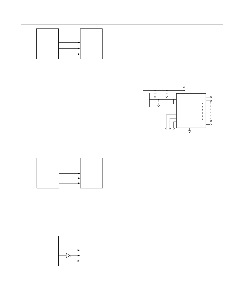
MICROWIRE to AD5308/AD5318/AD5328 Interface
Figure 14 shows an interface between the AD5308/AD5318/
AD5328 and any MICROWIRE compatible device. Serial data
is shifted out on the falling edge of the serial clock, SK, and is
clocked into the AD5308/AD5318/AD5328 on the rising edge
of SK, which corresponds to the falling edge of the DAC’s SCLK.
DIN
SCLK
SYNC
CS
SK
SO
MICROWIRE
*
*
ADDITIONAL PINS OMITTED FOR CLARITY
AD5308/
AD5318/
AD5328
*
Figure 14. MICROWIRE to AD5308/AD5318/
AD5328 Interface
APPLICATIONS
Typical Application Circuit
The AD5308/AD5318/AD5328 can be used with a wide range
of reference voltages where the devices offer full, one-quadrant
multiplying capability over a reference range of 0.25 V to V
DD
.
More typically, these devices are used with a fixed, precision
reference voltage. Suitable references for 5 V operation are the
AD780, ADR381, and REF192 (2.5 V references). For 2.5 V
operation, a suitable external reference would be the AD589
and AD1580 (1.2 V band gap references). Figure 15 shows a
typical setup for the AD5308/AD5318/AD5328 when using an
external reference.
1 F
V
REF
ABCD
V
REF
EFGH
AD5308/AD5318/
AD5328
V
OUT
V
IN
0.1 F
10 F
SCLK
DIN
SYNC
GND
V
OUT
A
V
OUT
B
SERIAL
INTERFACE
AD780/ADR3811/REF192
WITH V
= 5V OR
AD589/AD1580 WITH
V
DD
= 2.5V
V
DD
= 2.5V TO 5.5V
EXT
REF
V
OUT
H
V
OUT
G
Figure 15. AD5308/AD5318/AD5328 Using a 2.5 V
External Reference
Driving V
DD
from the Reference Voltage
If an output range of 0 V to V
DD
is required when the reference
inputs are configured as unbuffered, the simplest solution is to
connect the reference input to V
DD
. As this supply may be noisy
and not very accurate, the AD5308/AD5318/AD5328 may be
powered from a voltage reference. For example, using a 5 V
reference, such as the REF195, will work because the REF195
will output a steady supply voltage for the AD5308/AD5318/
AD5328. The typical current required from the REF195 is a
1
μ
A supply current and
≈
112
μ
A into the reference inputs (if
unbuffered); this is with no load on the DAC outputs. When the
DAC outputs are loaded, the REF195 also needs to supply the
current to the loads. The total current required (with a 10 k
load on each output) is
+
The load regulation of the REF195 is typically 2.0 ppm/mA,
which results in an error of 10.4 ppm (52
μ
V) for the 5.22 mA
current drawn from it. This corresponds to a 0.003 LSB error at
eight bits and 0.043 LSB error at 12 bits.
Bipolar Operation Using the AD5308/AD5318/AD5328
The AD5308/AD5318/AD5328 have been designed for single-
supply operation, but a bipolar output range is also possible
using the circuit in Figure 16. This circuit will give an output
voltage range of
±
5 V. Rail-to-rail operation at the amplifier
output is achievable using an AD820, the AD8519, or an OP196
as the output amplifier.
1.
8 5
10
5.
/
mA
V
k
mA
)
=
相关PDF资料 |
PDF描述 |
|---|---|
| AD530D | Integtated Circuit Multiplier,Divider,Squarer,Square Rooster |
| AD530H | 14 Bit 80 MSPS Analog-to-Digital Converter 52-QFP -40 to 85 |
| AD530J | Integtated Circuit Multiplier,Divider,Squarer,Square Rooster |
| AD530K | 14 Bit 80 MSPS Analog-to-Digital Converter 52-QFP -40 to 85 |
| AD530L | Integtated Circuit Multiplier,Divider,Squarer,Square Rooster |
相关代理商/技术参数 |
参数描述 |
|---|---|
| AD5318ARU | 功能描述:IC DAC 10BIT OCTAL W/BUF 16TSSOP RoHS:否 类别:集成电路 (IC) >> 数据采集 - 数模转换器 系列:- 标准包装:47 系列:- 设置时间:2µs 位数:14 数据接口:并联 转换器数目:1 电压电源:单电源 功率耗散(最大):55µW 工作温度:-40°C ~ 85°C 安装类型:表面贴装 封装/外壳:28-SSOP(0.209",5.30mm 宽) 供应商设备封装:28-SSOP 包装:管件 输出数目和类型:1 电流,单极;1 电流,双极 采样率(每秒):* |
| AD5318ARU-REEL7 | 功能描述:IC DAC 10BIT OCTAL W/BUF 16TSSOP RoHS:否 类别:集成电路 (IC) >> 数据采集 - 数模转换器 系列:- 标准包装:2,400 系列:- 设置时间:- 位数:18 数据接口:串行 转换器数目:3 电压电源:模拟和数字 功率耗散(最大):- 工作温度:-40°C ~ 85°C 安装类型:表面贴装 封装/外壳:36-TFBGA 供应商设备封装:36-TFBGA 包装:带卷 (TR) 输出数目和类型:* 采样率(每秒):* |
| AD5318ARUZ | 功能描述:IC DAC 10BIT OCTAL W/BUF 16TSSOP RoHS:是 类别:集成电路 (IC) >> 数据采集 - 数模转换器 系列:- 产品培训模块:Lead (SnPb) Finish for COTS Obsolescence Mitigation Program 标准包装:50 系列:- 设置时间:4µs 位数:12 数据接口:串行 转换器数目:2 电压电源:单电源 功率耗散(最大):- 工作温度:-40°C ~ 85°C 安装类型:表面贴装 封装/外壳:8-TSSOP,8-MSOP(0.118",3.00mm 宽) 供应商设备封装:8-uMAX 包装:管件 输出数目和类型:2 电压,单极 采样率(每秒):* 产品目录页面:1398 (CN2011-ZH PDF) |
| AD5318ARUZ | 制造商:Analog Devices 功能描述:IC DAC 10BIT 167KSPS 16TSSOP |
| AD5318ARUZ-REEL7 | 功能描述:IC DAC 10BIT OCTAL W/BUF 16TSSOP RoHS:是 类别:集成电路 (IC) >> 数据采集 - 数模转换器 系列:- 产品培训模块:Lead (SnPb) Finish for COTS Obsolescence Mitigation Program 标准包装:50 系列:- 设置时间:4µs 位数:12 数据接口:串行 转换器数目:2 电压电源:单电源 功率耗散(最大):- 工作温度:-40°C ~ 85°C 安装类型:表面贴装 封装/外壳:8-TSSOP,8-MSOP(0.118",3.00mm 宽) 供应商设备封装:8-uMAX 包装:管件 输出数目和类型:2 电压,单极 采样率(每秒):* 产品目录页面:1398 (CN2011-ZH PDF) |
发布紧急采购,3分钟左右您将得到回复。